Transistors
Publication date: October 2008 SJC00413AED 1
This product complies with the RoHS Directive (EU 2002/95/EC).
2SB0710ASilicon PNP epitaxial planar type
For general amplification
Complementary to 2SD0602A
Features
Large collector current IC
Mini type package, allowing downsizing of the eq uipment and automatic
insertion through the tape packing
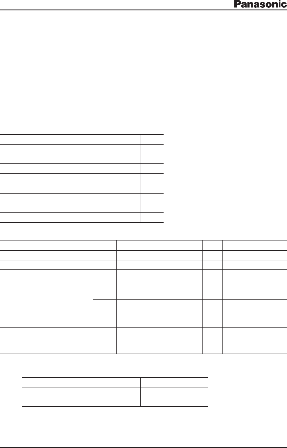
Absolute Maximum Ratings Ta = 25°C
Parameter Symbol Rating Unit
Collector-base voltage (Emitter open) VCBO -60 V
Collector-emitter voltage (Base open) VCEO -50 V
Emitter-base voltage (Collector open) VEBO -5V
Collector current IC- 0.5 A
Peak collector current ICP -1A
Collector power dissipation PC200 mW
Junction temperature Tj150 °C
Storage temperature Tstg -55 to +150 °C
Electrical Characteristics Ta = 25°C±3°C
Parameter Symbol Conditions Min Typ Max Unit
Collector-base voltage (Emitter open) VCBO IC = -10 mA, IE = 0 -60 V
Collector-emitter voltage (Base open) VCEO IC = -10 mA, IB = 0 -50 V
Emitter-base voltage (Collector open) VEBO IE = -10 mA, IC = 0 -5V
Collector-base cutoff current (Emitter open) ICBO VCB = -20 V, IE = 0 - 0.1 mA
Forward current transfer ratio *1hFE1 *2VCE = -10 V, IC = -150 mA 85 340
hFE2 VCE = -10 V, IC = -500 mA 40
Collector-emitter saturation voltage *1VCE(sat) IC = -300 mA, IB = -30 mA - 0.35 - 0.60 V
Base-emitter saturation voltage *1VBE(sat) IC = -300 mA, IB = -30 mA -1.1 -1.5 V
Transition frequency fTVCB = -10 V, IE = 50 mA, f = 200 MHz 200 MHz
Collector output capacitance
(Common base, input open circuited) Cob VCB = -10 V, IE = 0, f = 1 MHz 6 15 pF
Note) 1. Measuring methods are based on JAPANESE INDUSTRIAL STANDARD JIS C 7030 measuring methods for transistors.
2. *1: Pulse measurement
*2: Rank classification
Rank Q R S No-rank
hFE1 85 to 170 120 to 240 170 to 340 85 to 340
Marking symbol DQ DR DS D
Product of no-rank is not classified and have no indication for rank.
Package
Code
Mini3-G1
Pin Name
1: Base
2: Emitter
3: Collector