Transistors
Publication date : October 2008 SJC00422AED 1
This product complies with the RoHS Directive (EU 2002/95/EC).
2SC2406Silicon NPN epitaxial planar type
For low-frequency and low-noise amplification
Complementary to 2SA1035
Features
Low noise voltage NV
High forward current transfer ratio hFE
Mini type package, allowing downsizing of the equipment and automatic
insertion through the tape packing.
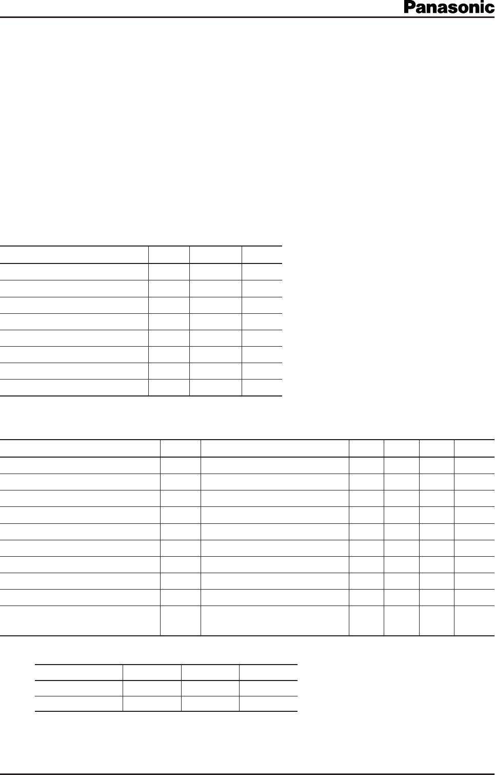
Absolute Maximum Ratings Ta = 25°C
Parameter Symbol Rating Unit
Collector-base voltage (Emitter open) VCBO 55 V
Collector-emitter voltage (Base open) VCEO 55 V
Emitter-base voltage (Collector open) VEBO 5 V
Collector current IC50 mA
Peak collector current ICP 100 mA
Collector power dissipation PC200 mW
Junction temperature Tj150 °C
Storage temperature Tstg –55 to +150 °C
Electrical Characteristics Ta = 25°C±3°C
Parameter Symbol Conditions Min Typ Max Unit
Collector-base voltage (Emitter open) VCBO IC = 10 mA, IE = 0 55 V
Collector-emitter voltage (Base open) VCEO IC = 2 mA, IB = 0 55 V
Emitter-base voltage (Collector open) VEBO IE = 10 mA, IC = 0 5 V
Base-emitter voltage VBE VCE = 1 V, IC = 100 mA 0.7 1.0 V
Collector-base cutoff current (Emitter open) ICBO VCB = 10 V, IE = 0 0.1 mA
Collector-emitter cutoff current (Base open) ICEO VCB = 10 V, IB = 0 1 mA
Forward current transfer ratio *hFE VCE = 5 V, IC = 2 mA 180 700
Collector-emitter saturation voltage VCE(sat) IC = 100 mA, IB = 10 mA 0.6 V
Transition frequency fTVCB = 5 V, IE = –2 mA, f = 200 MHz 200 MHz
Noise voltage
NV VCB = 10 V, IC = 1 mA, GV = 80 dB,
Rg = 100 kΩ, Function = FLAT 110 mV
Note) 1. Measuring methods are based on JAPANESE INDUSTRIAL STANDARD JIS C 7030 measuring methods for transistors.
2. *: Rank classification
Rank R S T
hFE 180 to 360 260 to 520 360 to 700
Merking symbol TR TS TT
Package
Code
Mini3-G1
Pin Name
1. Base
2. Emitter
3. Collector