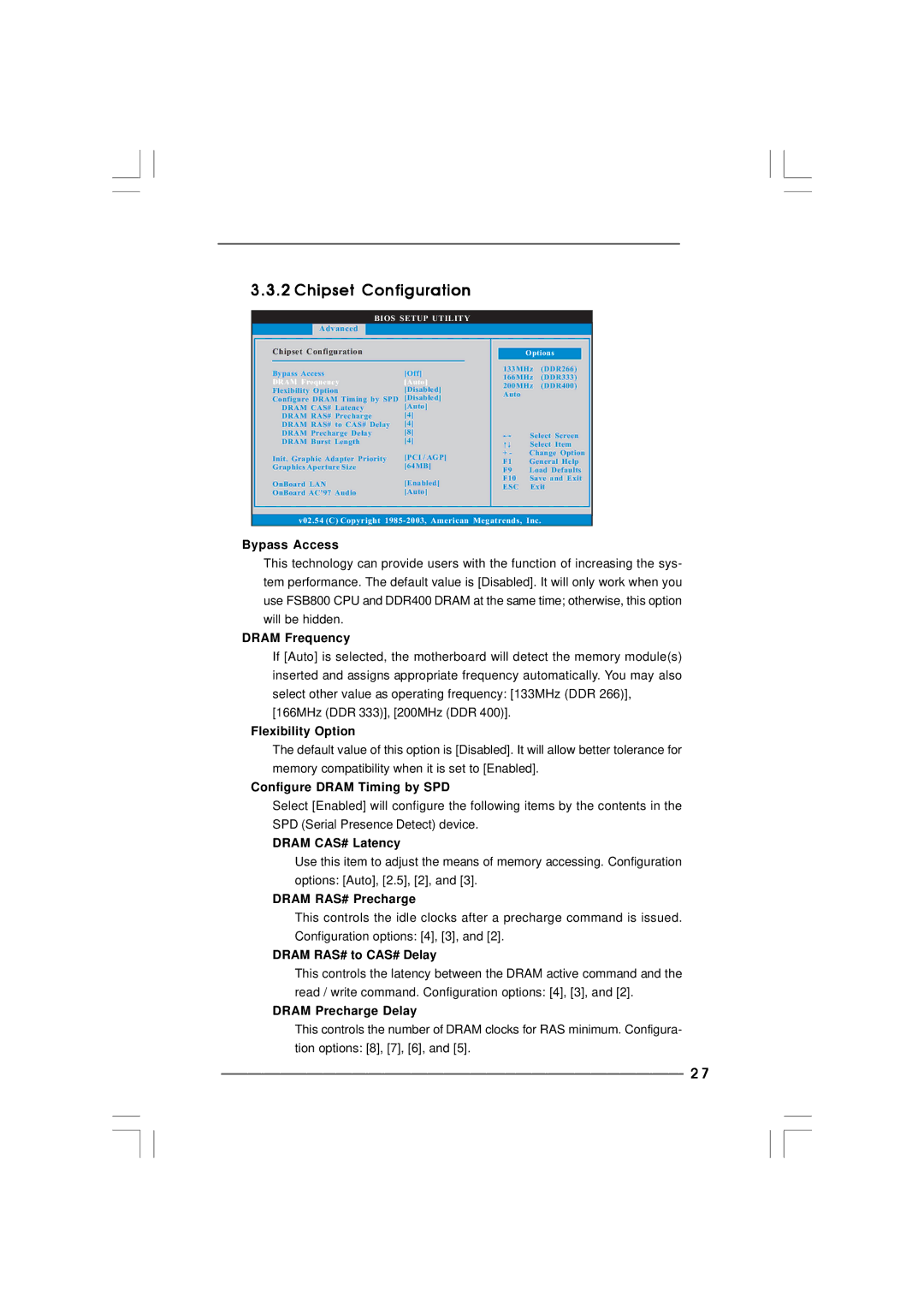
3.3.2 Chipset Configuration
BIOS SETUP UTILITY
Advanced
Chipset Configuration
Bypass Access | [Off] |
DRAM Frequency | [Auto] |
Flexibility Option | [Disabled] |
Configure DRAM Timing by SPD | [Disabled] |
DRAM CAS# Latency | [Auto] |
DRAM RAS# Precharge | [4] |
DRAM RAS# to CAS# Delay | [4] |
DRAM Precharge Delay | [8] |
DRAM Burst Length | [4] |
Init. Graphic Adapter Priority | [PCI / AGP] |
Graphics Aperture Size | [64MB] |
OnBoard LAN | [Enabled] |
OnBoard AC'97 Audio | [Auto] |
Options
133MHz (DDR266) 166MHz (DDR333) 200MHz (DDR400) Auto
| Select Screen |
| Select Item |
+ - | Change Option |
F1 | General Help |
F9 | Load Defaults |
F10 | Save and Exit |
ESC | Exit |
v02.54 (C) Copyright
Bypass Access
This technology can provide users with the function of increasing the sys- tem performance. The default value is [Disabled]. It will only work when you use FSB800 CPU and DDR400 DRAM at the same time; otherwise, this option will be hidden.
DRAM Frequency
If [Auto] is selected, the motherboard will detect the memory module(s) inserted and assigns appropriate frequency automatically. You may also select other value as operating frequency: [133MHz (DDR 266)], [166MHz (DDR 333)], [200MHz (DDR 400)].
Flexibility Option
The default value of this option is [Disabled]. It will allow better tolerance for memory compatibility when it is set to [Enabled].
Configure DRAM Timing by SPD
Select [Enabled] will configure the following items by the contents in the SPD (Serial Presence Detect) device.
DRAM CAS# Latency
Use this item to adjust the means of memory accessing. Configuration options: [Auto], [2.5], [2], and [3].
DRAM RAS# Precharge
This controls the idle clocks after a precharge command is issued. Configuration options: [4], [3], and [2].
DRAM RAS# to CAS# Delay
This controls the latency between the DRAM active command and the read / write command. Configuration options: [4], [3], and [2].
DRAM Precharge Delay
This controls the number of DRAM clocks for RAS minimum. Configura- tion options: [8], [7], [6], and [5].
2 7
