AN2309
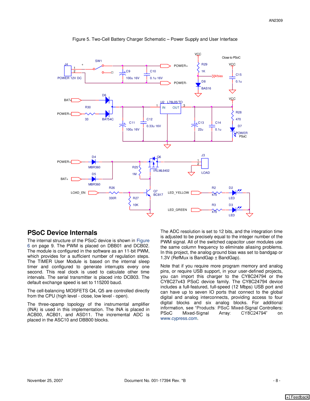
Figure 5. Two-Cell Battery Charger Schematic – Power Supply and User Interface
SW1
J4+
1
2
POWER 12V DC
D6
BAT+![]()
![]()
![]()
![]()
![]()
R30
POWER+![]()
![]()
![]()
![]()
![]()
![]()
![]()
![]()
![]()
![]()
33BAT54C
D4
POWER+![]()
![]()
![]()
![]()
![]()
![]()
![]() MBR360
MBR360
D5
BAT+
MBR360
R26
LOAD_EN
330R
POWER+
+ C9 |
| C10 | |
|
|
|
|
|
|
|
|
100u 16V |
| 0.1u 16V | |
POWER-
U2 L78L05/TO
13
IN OUT
C12
+ C11
0.33u 16V
100u 16V
Q6
R25 ![]()
![]()
![]()
![]()
![]()
![]() IRLML6402
IRLML6402
1M
Q7 LED_YELLOW BC817
R27
10K
LED_GREEN
VCC
| Close to PSoC | |
R29 |
| VCC |
1K |
|
|
| Vbias | C15 |
|
| |
D8 |
| 0.1u |
BAS16 |
|
|
|
| VCC |
|
| R28 |
|
| 470 |
+ C13 | C14 | D7 |
|
| |
22u | 0.1u |
|
|
| POWER |
|
| PSoC |
J3
1
2
LOAD
R2 | D2 |
470 |
|
LED
R3 D3
470
LED
PSoC Device Internals
The internal structure of the PSoC device is shown in Figure 6 on page 9. The PWM is placed on DBB01 and DCB02. The module is configured in the software as an
The
The
The ADC resolution is set to 12 bits, and the integration time is adjusted to be precisely equal to the integer number of the PWM signal. All of the switched capacitor user modules use the same column frequency to eliminate aliasing problems. In this project, the analog ground bias was set to bandgap or 1.3V (RefMux is BandGap ± BandGap).
Note that if you require more program memory and analog pins, or require USB support, in your
PSoC
November 25, 2007 | Document No. | - 8 - |
[+] Feedback
