Warning


Please read this instruction sheet carefully before use.
DO NOT touch any terminal when the power is switched on. Switch off the power before wiring.
DVP06XA-H2 is an OPEN-TYPE device and therefore should be installed in an enclosure free of airborne dust, humidity, electric shock and vibration. The enclosure should prevent non-maintenance staff from operating the device (e.g. key or specific tools are required to open the enclosure) in case danger and damage on the device may occur.
DO NOT connect input AC power supply to any of the I/O terminals; otherwise serious damage may occur. Check all the wiring again before switching on the power.
DO NOT touch the internal circuit for 1 minute after the power is switched off.
Make sure the ground terminal  is correctly grounded in order to prevent electromagnetic interference.
Introduction
Model Explanation & Peripherals
Thank you for choosing Delta DVP series PLC. DVP06XA-H2 is able to receive 4 points of analog input signals (voltage or current) and convert them into 12-bit digital signals. DVP06XA-H2 receives 2 groups of 12-bit digital data from PLC MPU and converts them into 2 points of analog signal for output (in voltage/current).
You can select voltage or current input by wiring. Range of voltage input: ±10V DC (resolution: 5mV).
Range of current input: ±20mA (resolution: 20µA).
You can also select voltage or current output by wiring. Range of voltage output: 0V ~ +10V DC
(resolution: 2.5mV), Range of current output: 0mA ~ 20mA (resolution: 5µA).
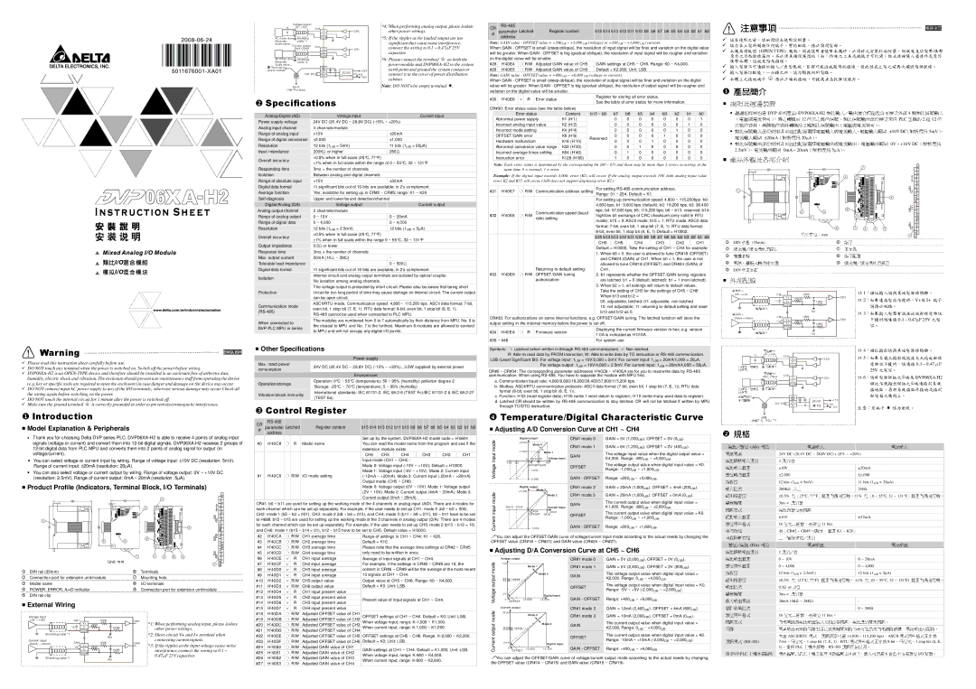
Product Profile (Indicators, Terminal Block, I/O Terminals)
| | 24V |
| RS- | 0V D |
| 485 | D - |
| | + |
CH CH 1 | V + V + I |
| 2 | + |
| | I + |
| | V CO M |
| CH 4 | + |
CH 3 | I + V + I |
| | CO + |
| | M V |
CH | | + |
CH | V + |
5 | I + |
Other Specifications
Power supply
| Max. rated power | 24V DC (20.4V DC ~ 28.8V DC) (-15% ~ +20%)., 3.5W supplied by external power |
| consumption |
| |
| | Environment |
| Operation/storage | Operation: 0°C ~ 55°C (temperature); 50 ~ 95% (humidity); pollution degree 2 |
| Storage: -25°C ~ 70°C (temperature); 5 ~ 95% (humidity) |
| Vibration/shock immunity | International standards: IEC 61131-2, IEC 68-2-6 (TEST Fc)/IEC 61131-2 & IEC 68-2-27 |
| (TEST Ea) |
Control Register
CR | RS-485 | Latched | Register content | b15 | b14 | b13 | b12 | b11 | b10 | b9 | | b8 | b7 | b6 | b5 | b4 | b3 | b2 | b1 | b0 |
parameter | |
# | |
address | | | | | | | | | | | | | | | | | | | | |
| | | | | Set up by the system. DVP06XA-H2 model code = H’6604 |
#0 | H’40C8 | | R | Model name | You can read the model name from the program and see if the |
| | | | | extension module exists. | | | | | | | | |
| | | | | CH6 | CH5 | CH4 | | | CH3 | CH2 | CH1 |
| | | | | Input mode (CH1 ~ CH4) : | | | | | | | | |
| | | | | Mode 0: Voltage input (-10V ~ +10V); Default = H’0000. |
| | | | | Mode 1: Voltage input (-6V ~ +10V). Mode 2: Current input |
#1 | H’40C9 | ○ | R/W | I/O mode setting | (-12mA ~ +20mA). Mode 3: Current input (-20mA ~ +20mA) |
| | | | | Output mode (CH5 ~ CH6) : | | | | | | | | |
| | | | | Mode 0: Voltage output (0V ~ 10V). Mode 1: Voltage output |
| | | | | (2V ~ 10V). Mode 2: Current output (4mA ~ 20mA). Mode 3: |
| | | | | Current output (0mA ~ 20mA). | | | | | | | | |
CR#1: b0 ~ b11 are used for setting up the working mode of the 4 channels in analog input (A/D). There are 4 modes for
each channel which can be set up separately. For example, if the user needs to set up CH1: mode 0 (b2 ~ b0 = 000),
CH2: mode 1 (b5 ~ b3 = 001), CH3: mode 2 (b8 ~ b6 = 010), and CH4: mode 3 (b11 ~ b9 = 011), b0 ~ b11 have to be set to H688. b12 ~ b15 are used for setting up the working mode of the 2 channels in analog output (D/A). There are 4 modes for each channel which can be set up separately. For example, if the user needs to set up CH5: mode 2 (b13 ~ b12 = 10) and CH6: mode 1 (b15 ~ b14 = 01), b12 ~ b15 have to be set to CH5. Default value = H’0000.
#2 | H’40CA | | R/W | CH1 average time | Range of settings in CH1 ~ CH4: K1 ~ K20. |
#3 | H’40CB | | R/W | CH2 average time | Default = K10. |
#4 | H’40CC | | R/W | CH3 average time | Please note that the average time settings at CR#2 ~ CR#5 |
#5 | H’40CD | ○ | R/W | CH4 average time | only need to be written in once. |
| | | | | |
| | | | | |
| | | | | |
| | | | | |
| | | | | |
| | | | | |
| | | | | |
| | | | | |
| | | | | |
| | | | | |
| | | | | |
| | | | | |
| | | | | |
| | | | | |
| | | | | |
| | | | | |
| | | | | |
| | | | | |
| | | | | |
| | | | | |
Symbols: : Latched (when written in through RS-485 communication). : Non-latched.
R: Able to read data by FROM instruction, W: Able to write data by TO instruction or RS-485 communication. LSB (Least Significant Bit): For voltage input: 1LSB = 10V/2,000 = 5mV. For current input: 1LSB = 20mA/1,000 = 20µA.
For voltage output: 1LSB = 10V/4,000 = 2.5mV. For current input: 1LSB = 20mA/4,000 = 50µA.
CR#0 ~ CR#34: The corresponding parameter addresses H’40C8 ~ H’40EA are for you to read/write data by RS-485 communication. When using RS-485, You have to separate the module with MPU first.
a. Communication baud rate: 4,800/9,600/19,200/38,400/57,600/115,200 bps.
b. Modbus ASCII/RTU communication protocols: ASCII data format (7-bit, even bit, 1 stop bit (7, E, 1)); RTU data format (8-bit, even bit, 1 stop bit (8, E, 1)).
c. Function: H’03 (read register data); H’06 (write 1 word datum to register); H’10 (write many word data to register).
d. Latched CR should be written by RS-485 communication to stay latched. CR will not be latched if written by MPU through TO/DTO instruction.
Temperature/Digital Characteristic Curve
Adjusting A/D Conversion Curve at CH1 ~ CH4
mode | | Digital output | | CR#1 mode 0 | GAIN = 5V (1,000LSB). OFFSET = 0V (0LSB). |
| | | |
| +2,000 | Mode 0 | | | |
| | | CR#1 mode 1 | GAIN = 6V (1,200LSB). OFFSET = 2V (400LSB). |
| | | |
| +1,000 | | Mode 1 | | |
input | | | | The voltage input value when the digital output value = |
| | | | GAIN |
| 0 | 2V 5V 6V | Voltage input | K4,000. Range: -800LSB~ +4,000LSB. |
| |
Voltage | -10 V -6 V | | | 10 V | | The voltage output value when digital input value = K0. |
| | OFFSETGAIN | OFFSET |
| | | | Range: -1,000LSB~ +1,000LSB. |
| | -1,000 | | |
| | -2,0 00 | | GAIN - OFFSET | Range: +200LSB ~ +3,000LSB. |
| ○ | Digital output | | CR#1 mode 2 | ╳ |
| | Mode 3 | GAIN = 20mA (1,000LSB). OFFSET = 4mA (200LSB). |
mode | | +1,000 | | | | |
| | | Mode 2 | CR#1 mode 3 | GAIN = 20mA (1,000LSB). OFFSET = 0mA (0LSB). |
| | | | GAIN | The current output value when digital input value = |
input | -20m A -12m A 0 | | Current input | K1,000. Range: -800LSB~ +2,600LSB. |
| |
| | 4mA | 20mA | | The current output value when digital input value = K0. |
| | OFFS ET | GAI N | OFFSET |
Current | | | | | Range: -1,000LSB~ +1,000LSB. |
| | | | |
| | -1,0 00 | | GAIN - OFFSET | Range: +200LSB ~ +1,600LSB. |
You can adjust the OFFSET/GAIN curve of voltage/current input mode according to the actual needs by changing the OFFSET value (CR#18 ~ CR#21) and GAIN value (CR#24 ~ CR#27).
Adjusting D/A Conversion Curve at CH5 ~ CH6
| | | | | | | | | | | | | | | 4 | | | | | |
| | | *5 | 0V~+10V | | CH5 | | | | | | | | | | | | |
| | | | | | | V+ | | | | | | 5 | | | | | |
| | | | | | | | | | | | CH5 | | | | | | |
| | | | | | | | | I+ | | | | | | | | 負載之輸出端漣波太0.1大~造成0.47配線F |
| | | | 電壓輸出*1 | | | CO M | | | | | | | |
| | | | | | | | | | | | | | | | 25V | | | | |
| | | | 0mA~20mA | | CH | | | | | | | 6 | | | | DVP06XA-H2 |
比變例頻閥器 | ...、記錄器 | | | | | | V+ | | | | CH | | | | |
| | | | | | | | | I+ | | | | | | | | | | | |
| | | | | | | | | COM | | | | | | | | | | | |
| | | | | 流 | * | | 6 | | | | | | | | | | | | |
| | | | | | | | | | | | | | | | 接地點信,號再輸出將模系組統之接點端作連接接地到或系接統到 |
| | | | | | | | | 24+ | | DC/DC | | +15 V | | | | | | | |
| | | | | | 24V DC | | | 6 | | | | | | | |
接組至之電源端模 | | | | 24- | | | | AG | | | | | | | |
外部配線 | | | | | | | | | | -15 V | | | 類比 | | 請與其他電源線隔離。 | |
| | | | | | | | | | | | | |
| | | | | | | | | | | | | | | | | 連接 流信號時, | 及 | |
| | (AD) | | | | | | | | | | | | | 請務必短路。 | | |
| | | | | | | | | | | | | | | 入電 | | |
| | | 隔離線 | | | 24V DC (20.4V DC ~ 28.8V DC) (-15% ~ +20%) | | | | |
| | | | | | 干擾時請連接 | | |
| | | | | | | | | | | | | | | |
| | | | | 4 | | / | | | | | | | 容。 | | | | |
| | | | | | | | | | | | | | | | | |
| | | | | ±10V | | | | | | ±20mA | | | | |
| | | | | | | | | | | | | | | | | | |
| | | | | | | ±2,000 | | | | | ±1,000 | | | | | |
| | | | | | | 12 bits (1LSB = 5mV) | | | 11 bits (1LSB | = 20µA) | | |
| | | | | | | 200K | | | | | 250 | | 輸出請與其他電源線隔離。 | |
| | | | | | | ±0.5% | | 25°C, 77°F | | | ±1% | | 如0 果~ 55°C, 32 ~ 131°F | | μ |
| | | | | | | 3ms × | | | | | | | | 受雜訊干擾時,請連接 | |
| | | | | | | | | | | | | | | | | 之電容。 | | |
| | | | | | | ±15V | | | | | | | :請將電源模組之 端及 | | |
| | | | | | | | | | | | ±32mA | | | | |
| | | | | 隔離線 4 | | | | | | | | | | 類比 | | | | |
| | | | | 16 | | | 轉換器 | 11 bits | | | 配電箱之機殼上。 | | |
| | | | | | | | CR#2 ~ CR#5 | | K1 ~ K20 | | | | |
| | | | | | | | | | | | | | | | |
| | (DA) | 接地 | 以下) | | | | | | | | 注意:空端子 | 請勿配線。 | | |
| | | | 2 | | | 電壓輸出 | | | | | | 電流輸出 | | |
| | | | | | | | | | | | | | | | | |
| | (接地阻抗 100 | | | | | | | | | | | | | | |
規格 | | | 部份 | | | | | 電壓輸入 | | | | | | 電流輸入 | | |
類比╱數位 | | | | | | | | | | | | | |
電源電壓 | | | | | | | | 通道 台 | | | | | | | | | | | |
訊號輸入通道 | | | | | | | | | | | | | | | |
類比輸入 | | | | | | | | | | | | | | | | | | | | |
數位轉換 | | | | | | | | | | | | | | | | | | | | |
解析度 | | | | | | | | | | | | | | | | | | | | |
| | | 6 | I |
| Unit: mm | | 8 | + CO |
| | | M |
1 | DIN rail (35mm) | 6 | Terminals | |
2 | Connection port for extension unit/module | 7 | Mounting hole | |
3 | Model name | 8 | I/O terminals | |
4 | POWER, ERROR, A D indicator | 9 | Connection port for extension unit/module | |
5DIN rail clip
External Wiring
Voltage input | | | | | | | |
-10V ~ +10V | CH1 | V+ | 100K | | | CH1 | *1: When performing analog input, please isolate |
| | 250 | | | |
| *3 | I+ | | | |
| | | 100K | | other power wirings. |
| | CO M | | | | |
| | | | | | |
Shielding cable *1 | | | | | | | *2: Short-circuit V+ and I+ terminal when |
| | | | AG | | | connecting current signals. |
Current input | CH4 | | 100K | | | |
-20mA ~ +20mA | V+ | | | CH4 | *3: If the ripples at the input voltage cause noise |
| *2 | 250 | | | |
| I+ | | | |
| | | | 100K | | interference,connect the wiring to 0.1 ~ |
| | CO M | | | | |
| | | | | | | 0.47µF 25V capacitor. |
| #6 | H’40CE | ╳ | R | CH1 input average | Average of input signals at CH1 ~ CH4. |
| #7 | H’40CF | R | CH2 input average | For example, if the settings in CR#2 ~ CR#5 are 10, the |
| #8 | H’40D0 | R | CH3 input average | content in CR#6 ~ CR#9 will be the average of the most recent |
| #9 | H’40D1 | R | CH4 input average | 10 signals at CH1 ~ CH4. |
| #10 | H’40D2 | R/W | CH5 output value | Output value at CH5 ~ CH6. Range: K0 ~ K4,000. |
| #11 | H’40D3 | R/W | CH6 output value | Default = K0. Unit: LSB. |
| #12 | H’40D4 | R | CH1 input present value | |
| #13 | H’40D5 | R | CH2 input present value | Present value of input signals at CH1 ~ CH4. |
| #14 | H’40D6 | R | CH3 input present value |
| |
| #15 | H’40D7 | R | CH4 input present value | |
| #18 | H’40DA | | R/W | Adjusted OFFSET value of CH1 | OFFSET settings at CH1 ~ CH4. Default = K0; Unit: LSB. |
| #19 | H’40DB | | R/W | Adjusted OFFSET value of CH2 | When voltage input, range: K-1,000 ~ K1,000. |
| #20 | H’40DC | | R/W | Adjusted OFFSET value of CH3 | When current input, range: K-1,000 ~ K1,000. |
| #21 | H’40DD | | R/W | Adjusted OFFSET value of CH4 | |
| #22 | H’40DE | | R/W | Adjusted OFFSET value of CH5 OFFSET settings at CH5 ~ CH6. Range: K-2,000 ~ K2,000. |
| #23 | H’40DF | | R/W | Adjusted OFFSET value of CH6 Default = K0; Unit: LSB. |
| #24 | H’40E0 | | R/W | Adjusted GAIN value of CH1 | GAIN settings at CH1 ~ CH4. Default = K1,000; Unit: LSB. |
| #25 | H’40E1 | | R/W | Adjusted GAIN value of CH2 |
| | When voltage input, range: K-800 ~ K4,000. |
| | | | | |
Current output mode Voltage output mode
Voltage output | | |
1 0 V | | | |
| | Mode 1 | |
| | | Mode 0 |
6 V | G AI N | | |
5 V | | |
2 V | | | Digital input |
| | |
0 | | +2,0 0 0 | +4,0 0 0 |
O FFS ET | | |
Current output | | |
20 mA | | | |
| | Mode 2 | |
| | | Mode 3 |
12 mA | G AI N | | |
10 mA | | |
4 m A | | | Digital input |
| | |
0 | O FFSE T | +2,0 00 | +4,0 00 |
| | |
CR#1 mode 0
CR#1 mode 1
GAIN
OFFSET
GAIN - OFFSET
CR#1 mode 2
CR#1 mode 3
GAIN
OFFSET
GAIN - OFFSET
GAIN = 5V (2,000LSB). OFFSET = 0V (0LSB).
GAIN = 6V (2,400LSB). OFFSET = 2V (800LSB).
The voltage output value when digital input value = K2,000. Range: 0LSB ~ +4,000LSB.
The voltage output value when digital input value = K0. Range: -5V ~ +5V (-2,000LSB ~ +2,000LSB).
Range: +400LSB ~ +6,000LSB.
GAIN = 12mA (2,400LSB). OFFSET = 4mA (800LSB).
GAIN = 10mA (2,000LSB). OFFSET = 0mA (0LSB).
The current output value when digital input value = K2,000. Range: 0LSB ~ +4,000LSB.
The current output value when digital input value = K0. Range: -10mA ~ +10mA (-2,000LSB ~ +2,000LSB).
Range: +400LSB ~ +6,000LSB.
| | 0 ~ 10V | | | | | | | 0 ~ 20mA | | |
| | 0 ~ 4,000 | | | | | | 0 ~ 4,000 | | |
| | 12 bits (1LSB = 2.5mV) | | | | 12 bits (1LSB = 5µA) | |
| | ±0.5% | | (25°C, 77°F) | | ±1% (0 ~ 55°C, 32 ~ 131°F) |
| | 0.5 or | | | | | | | | | | |
| | 3ms × | | | | | | | | | | | |
| | 20mA (1K ~ 2M) | | | | - | | | |
輸入阻抗 | | - | | | | 以上 | | | | | | 0 ~ 500 | | |
| 16 | | | | | 11 bits | | | | | | |
| | | | | | | )範圍內滿刻度時。(4,800 ~ 115,200在( | | )範圍內滿刻度時。 |
總和精密度 | | 7包-bit含 | ASCII/RTU在( | | bps) ASCII |
響應時間 (RS-485) | | | 通道數 | 1 stop bit (7, E, 1) RTU | | | | | 8-bit | 模式資料1格stop式固bit定(8,為 E, |
隔離方式 | | 1) | | | PLC | | | RS-485 | | | | | | |
| 類比與數位有隔離 | | | | | | | |
DVP-PLC | | | | | | | | | | 0 | | 7 | | 8 | I/O |
絕對 入 | | 有( | | | | | 可設定,範圍 | | ) | | | | |
平均功能 | | | | | | | | | | |
自我診斷功能 | 部份 | 上下極限偵測╱通道 | | | | | | | |
數位╱類比 | | 通道位元╱通在二更台道補數低 | ,有效位範圍內。滿刻度時。 | | | 在 | | 範圍內滿刻度時。 |
容最響輸總解類數許大應出和析比位時阻精訊負度資輸載間抗密出號料阻電度輸格範出抗流式圍通道 | | | | | |