
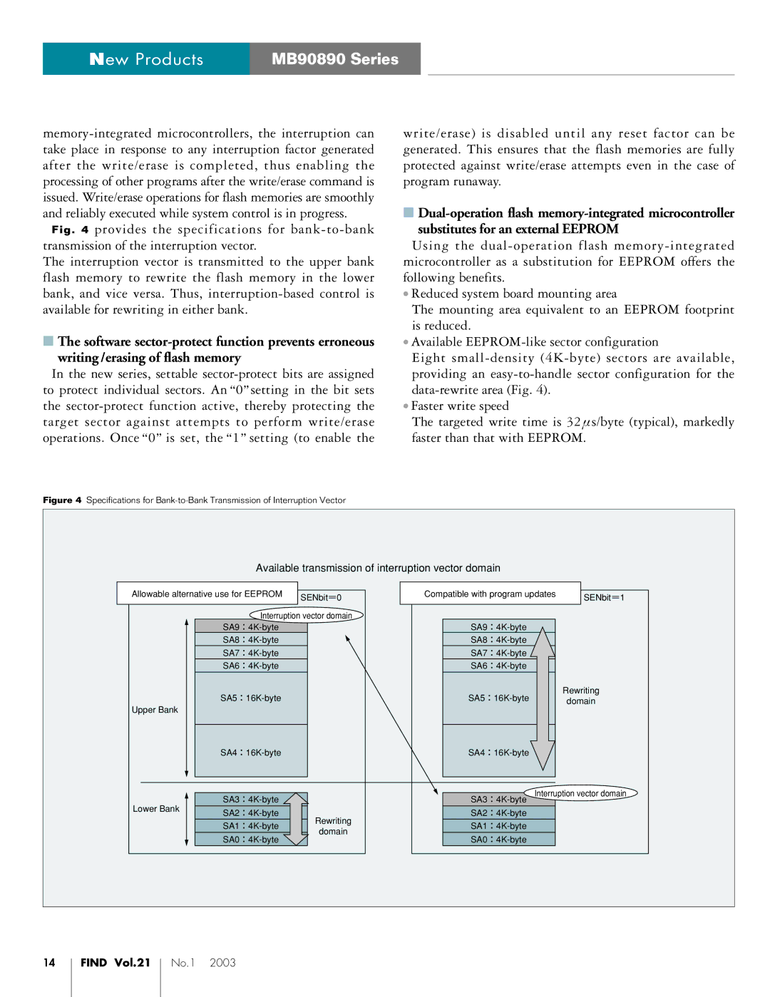
MB90890 specifications
The Fujitsu MB90890 is a high-performance microcontroller that stands out in the realm of embedded systems, particularly for automotive and industrial applications. Engineered with a focus on innovation, the MB90890 series showcases an array of characteristics that make it an ideal choice for various complex tasks.One of the principal features of the MB90890 microcontroller is its advanced processing capability. It incorporates a 32-bit FR (Fujitsu RISC) core, which is optimized for high-speed processing and efficiency. With a clock frequency reaching up to 80 MHz, it delivers exceptional performance for real-time applications, allowing embedded systems to execute tasks with minimal latency.
The MB90890 also boasts a rich set of peripherals designed to enhance its functionality. It offers multiple communication interfaces, including CAN (Controller Area Network), UART (Universal Asynchronous Receiver-Transmitter), and I2C (Inter-Integrated Circuit). These interfaces facilitate seamless communication with other components in an automotive or industrial system, promoting interoperability and flexibility.
In terms of memory, the microcontroller comes with various configuration options, including Flash and RAM. This flexibility allows developers to choose the right memory size according to the specific needs of their application. The integrated Flash memory allows for reprogramming, enabling software updates or modifications without the need for hardware changes.
Power efficiency is another standout characteristic of the MB90890. Its low-power design enables devices to operate for extended periods without the need for frequent recharging or battery replacement. This is especially critical in automotive applications, where power consumption considerations can significantly impact overall system performance and longevity.
Safety features are paramount in automotive applications, and the MB90890 addresses this need through its compliance with established safety standards. The architecture is designed to support error detection and fault isolation, essential for critical functions in safety-critical systems.
Moreover, the MB90890 microcontroller supports various development tools and software environments, streamlining the design and development process. With support for development kits, software libraries, and a comprehensive ecosystem, engineers find it easier to bring their projects to life.
In summary, the Fujitsu MB90890 microcontroller combines high performance, advanced features, and safety compliance, making it an excellent choice for modern embedded applications. Its robust architecture and flexible design cater to the needs of diverse industries, ensuring that it remains a reliable solution in a competitive marketplace.