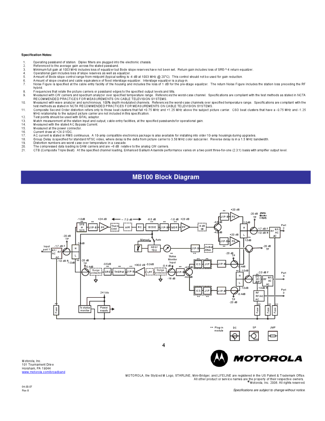
Motorola specifications MB100 Block Diagram, Specification Notes

Models: MB100

1 6
Download 6 pages 29.95 Kb
Page 4
Image 4
Specification Notes:

Specification Notes:

1.Operating passband of station. Diplex filters are plugged into the electronic chassis.

2.Referenced to the average gain across the stated passband.

3.Minimum full gain at 1003 MHz includes loss of equalizer but Bode slope reserves have not been set. Return gain includes loss of SRE-*-4 return equalizer.

4.Operational gain includes loss of slope reserves as well as equalizer.

5.Amount of Bode slope control range from midpoint (typical setting is -4 dB at 1003 MHz @ 20°C). This control should not be used for gain reduction.

6.Amount of slope created and cable equivalence of fixed interstage equalizer. Interstage equalizer is a plug-in.

7.Noise Figure is specified at the cable entry facility of the housing and includes the loss of 1 dB for the pre-stage equalizer. The return Noise Figure includes the station loss preceding the RF hybrid.

8.Frequencies that relate the picture carriers or passband edges to the specified output levels and tilts.

9.Measured with CW carriers and spectrum analyzer over specified temperature range. References the worst-case channel. Specifications are compliant with the test methods as stated in NCTA RECOMMENDED PRACTICES FOR MEASUREMENTS ON CABLE TELEVISION SYSTEMS.

10.Measured with wave analyzer and synchronous, 100% depth modulated channels. References the worst-case channels over specified temperature range. Specifications are compliant with the test methods as stated in NCTA RECOMMENDED PRACTICES FOR MEASUREMENTS ON CABLE TELEVISION SYSTEMS.

11.Composite Second Order distortion refers only to those beat clusters that fall +0.75 MHz and +1.25 MHz above the subject picture carrier. CSO beat clusters that have a -0.75 MHz and -1.25 MHz relationship to the subject picture carrier are not included in this specification.

12.Test points should be used with GFAL adaptor.

13.Match measurement at the station input and output, cable-entry facilities, at the specified passbands for operational gain.

14.Measured with the stated AC Bypass Current.

15.Measured at the power connector.

16.Current draw at +24.0 VDC.

17.AC current is stated in RMS continuous. A 10-amp compatible electronics package is also available for installing into older 10-amp housings during upgrades.

18.Group Delay is specified for standard NTSC video, where delay is the delta from picture carrier to 3.58 MHz color subcarrier. Reverse delay is in a 1.5 MHz bandwidth.

19.Distortion numbers are worst case over temperature in a cascade.

20.The compressed data loading is QAM carriers and are –6 dB relative to the analog CW carriers.

21.CTB (Composite Triple Beat). At the specified channel loading, Enhanced Gallium Arsenide performance varies on a two point three-for-one (2.3:1) basis with amplifier output level.

MB100 Block Diagram


**

+20 dB


-20 dB

(Status


JXP-B

PD


TP

Monitor


-1.0dB


+24 dB

~ -7.0 dB


-6.5 dB


-1.0 dB

+23 dB


Output)


**


**


**


**

**


-4.0 dB


-1.0dB


Port


SFE


Therm


BODE


PP

4 dB


or

JXP-B

PP

HPF

RC

JXP-B

MDR


H

-1.7 dB F


2


Cntrl


tilt


RF/


SCS


-4.0 dB


-20 dB


+20 dB

L

-1.0 dB R RF

AC


AC


**


TP


Manual

Auto


-1.0dB


JXP-B

PD

-1.0dB


Input

-1.7 dB F


**


-20 dB


H


ADU/


JXP-B

OnBrd


port 1

RF/


TP


RF


TDU


Atten

-20 dB


AC

L


**


**


AC


Status


**

**


TP


** -20 dB


Monitor


-1.0 dB R


Input


-1.0dB


TP


-0.5dB


+30.0 dB -0.3dB


ICS

JXP

JXP-B


-0.4dB

**

**

-0.4 dB

**

-4.0 dB

-0.4dB


**


SRE

THERM

JXP-B


LPF


JXP-B


**

-1.0dB

**-2.0 dB F


Port


H


-16 dB


-4.0 dB


DC/

RF

RF/


4


SP/


L


AC


JMP


AC


ICS

JXP

JXP-B


-1.0dB

-1.0dB R


Port


24 Vdc


RF


-0.4dB


3


**

**


RF/AC


TP


AC


**


-20 dB


**

**


**


To status


Power


Fuse


Fuse

Fuse

Fuse


monitor


supply


**

Plug-in

DC

SP

JMP


module


4

Motorola, Inc.

101 Tournament Drive

Horsham, PA 19044

www.motorola.com/broadband

MOTOROLA, the Stylized M Logo, STARLINE, Mini-Bridger, and LIFELINE are registered in the US Patent & Trademark Office. All other product or service names are the property of their respective owners.

© Motorola, Inc. 2006. All rights reserved.

04.03.07


Rev 8

Specifications are subject to change without notice.

Page 4
Image 4
Motorola specifications MB100 Block Diagram, Specification Notes