
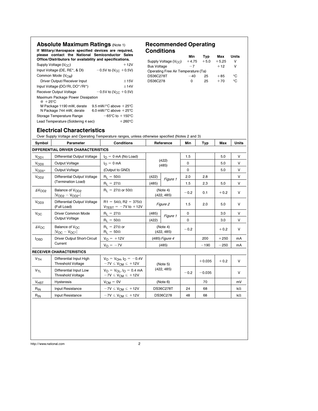
DS36C278 specifications
The National DS36C278 is a versatile and highly regarded dual/quad operational amplifier that has garnered attention for its impressive performance in various applications. As a member of the DS series, the DS36C278 integrates multiple features and technologies designed to meet the demands of both consumer and industrial electronics.One of the main features of the DS36C278 is its high-speed operation. It boasts a wide bandwidth and fast slew rates, which make it suitable for applications requiring rapid signal processing. The amplifier typically operates with a bandwidth of up to 16 MHz, allowing it to handle high-frequency signals with ease. Its slew rate can reach up to 9 V/µs, ensuring quick transitions and faithful signal reproduction, ideal for video and audio applications.
The DS36C278 is designed for versatility, allowing it to function as either a dual or quad amplifier. This flexibility enables designers to streamline layouts and reduce component counts in their circuit designs, ultimately saving space on printed circuit boards. The dual and quad configuration is particularly beneficial in modular systems where multiple signal paths are required.
Another defining characteristic of the DS36C278 is its low noise operation. With a low input-referred noise density, this amplifier excels in applications where signal integrity is paramount. The design effectively minimizes distortion and interference, making it suitable for precision instrumentation and sensitive audio applications.
The device operates on a wide supply voltage range, typically from ±4.5 to ±15 volts, making it compatible with different power supply standards. This flexibility enhances its applicability in various contexts, from handheld devices to stationary equipment.
Furthermore, the DS36C278 is characterized by its thermal stability. The amplifier features a construction that reduces susceptibility to temperature fluctuations, allowing consistent performance across varying environmental conditions. This characteristic is crucial for industrial applications where temperature controls may be less stringent.
In summary, the National DS36C278 is a high-performance operational amplifier featuring dual/quad capabilities, high speed, low noise operation, and robust thermal stability. Its wide supply voltage range adds to its adaptability, making it a valuable component in numerous electronic designs, from consumer electronics to industrial applications. With its blend of features and technologies, the DS36C278 continues to be a preferred choice for engineers and designers seeking reliable amplification solutions.