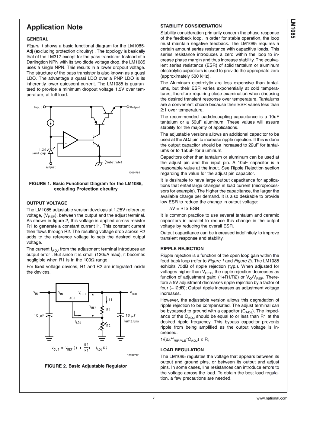
National Instruments LM1085 Series manual Application Note, General, Basic Adjustable Regulator

Models: LM1085 Series

1 13
Download 13 pages 40.45 Kb
Page 7
Image 7
Application Note

Application Note

GENERAL

Figure 1 shows a basic functional diagram for the LM1085- Adj (excluding protection circuitry) . The topology is basically that of the LM317 except for the pass transistor. Instead of a Darlingtion NPN with its two diode voltage drop, the LM1085 uses a single NPN. This results in a lower dropout voltage. The structure of the pass transistor is also known as a quasi LDO. The advantage a quasi LDO over a PNP LDO is its inherently lower quiescent current. The LM1085 is guaran- teed to provide a minimum dropout voltage 1.5V over tem- perature, at full load.

10094765

FIGURE 1. Basic Functional Diagram for the LM1085,

excluding Protection circuitry

OUTPUT VOLTAGE

The LM1085 adjustable version develops at 1.25V reference voltage, (VREF), between the output and the adjust terminal. As shown in figure 2, this voltage is applied across resistor R1 to generate a constant current I1. This constant current then flows through R2. The resulting voltage drop across R2 adds to the reference voltage to sets the desired output voltage.

The current IADJ from the adjustment terminal introduces an output error . But since it is small (120uA max), it becomes negligible when R1 is in the 100Ω range.

For fixed voltage devices, R1 and R2 are integrated inside the devices.

10094717

FIGURE 2. Basic Adjustable Regulator

STABILITY CONSIDERATION

Stability consideration primarily concern the phase response of the feedback loop. In order for stable operation, the loop must maintain negative feedback. The LM1085 requires a certain amount series resistance with capacitive loads. This series resistance introduces a zero within the loop to in- crease phase margin and thus increase stability. The equiva- lent series resistance (ESR) of solid tantalum or aluminum electrolytic capacitors is used to provide the appropriate zero (approximately 500 kHz).

The Aluminum electrolytic are less expensive than tantal- ums, but their ESR varies exponentially at cold tempera- tures; therefore requiring close examination when choosing the desired transient response over temperature. Tantalums are a convenient choice because their ESR varies less than 2:1 over temperature.

The recommended load/decoupling capacitance is a 10uF tantalum or a 50uF aluminum. These values will assure stability for the majority of applications.

The adjustable versions allows an additional capacitor to be used at the ADJ pin to increase ripple rejection. If this is done the output capacitor should be increased to 22uF for tantal- ums or to 150uF for aluminum.

Capacitors other than tantalum or aluminum can be used at the adjust pin and the input pin. A 10uF capacitor is a reasonable value at the input. See Ripple Rejection section regarding the value for the adjust pin capacitor.

It is desirable to have large output capacitance for applica- tions that entail large changes in load current (microproces- sors for example). The higher the capacitance, the larger the available charge per demand. It is also desirable to provide low ESR to reduce the change in output voltage:

∆V = ∆I x ESR

It is common practice to use several tantalum and ceramic capacitors in parallel to reduce this change in the output voltage by reducing the overall ESR.

Output capacitance can be increased indefinitely to improve transient response and stability.

RIPPLE REJECTION

Ripple rejection is a function of the open loop gain within the feed-back loop (refer to Figure 1 and Figure 2). The LM1085 exhibits 75dB of ripple rejection (typ.). When adjusted for voltages higher than VREF, the ripple rejection decreases as function of adjustment gain: (1+R1/R2) or VO/VREF. There- fore a 5V adjustment decreases ripple rejection by a factor of four (−12dB); Output ripple increases as adjustment voltage increases.

However, the adjustable version allows this degradation of ripple rejection to be compensated. The adjust terminal can be bypassed to ground with a capacitor (CADJ). The imped-

ance of the CADJ should be equal to or less than R1 at the desired ripple frequency. This bypass capacitor prevents

ripple from being amplified as the output voltage is in- creased.

1/(2π*fRIPPLE*CADJ) ≤ R1

LOAD REGULATION

The LM1085 regulates the voltage that appears between its output and ground pins, or between its output and adjust pins. In some cases, line resistances can introduce errors to the voltage across the load. To obtain the best load regula- tion, a few precautions are needed.

LM1085

7

www.national.com

Page 7
Image 7
National Instruments LM1085 Series Application Note, General, Basic Functional Diagram for the LM1085, Ripple Rejection