
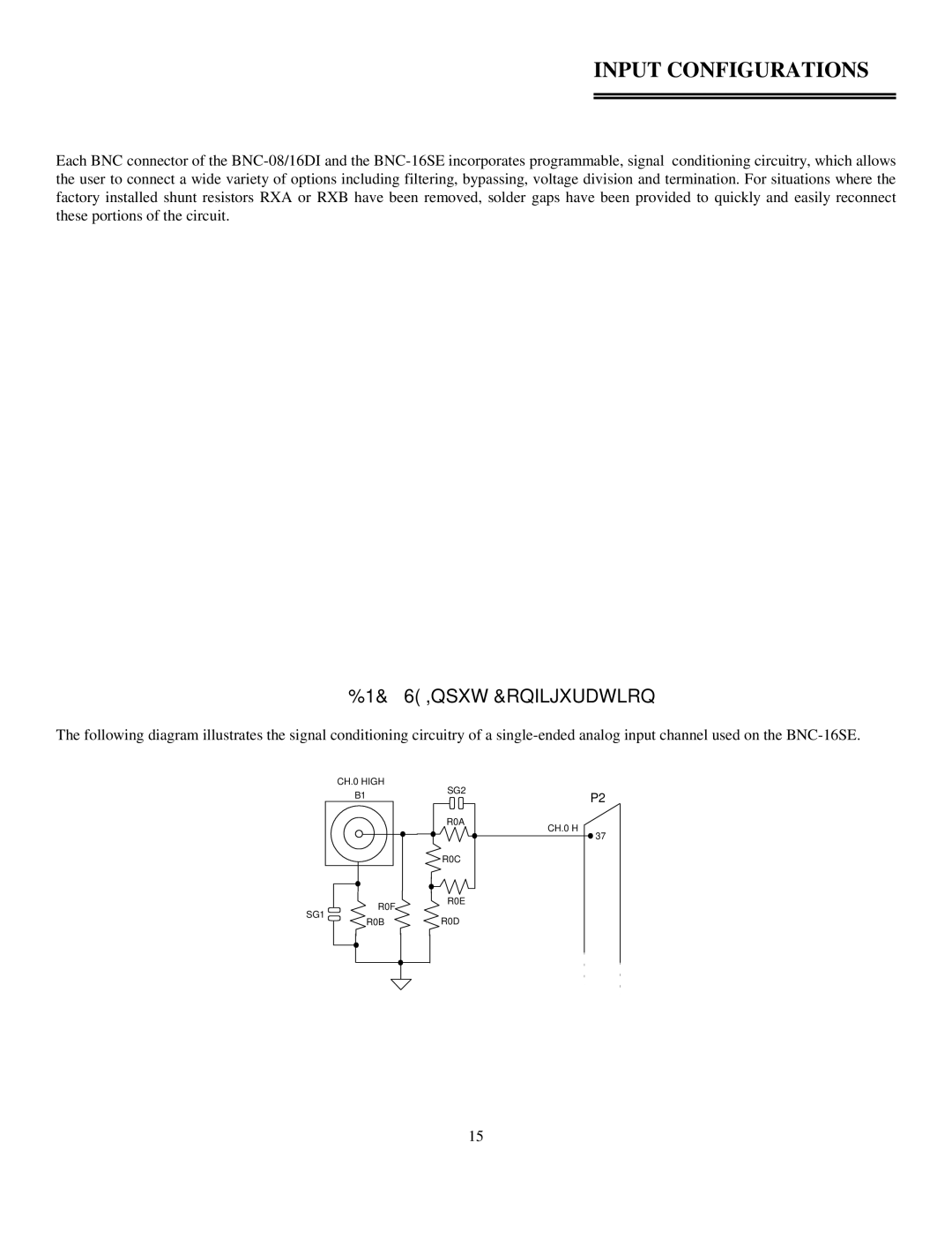
BNC-08DI, BNC-16DI, BNC-16SE, BNC-08DI specifications
Omega Engineering has made significant strides in industrial measurement and control solutions, particularly with their series of data acquisition and control devices, such as the BNC-08DI, BNC-08DI, BNC-16DI, and BNC-16SE. Each of these models represents advanced technology designed to meet various industrial applications, offering reliability, versatility, and ease of use.The BNC-08DI is a compact, high-performance data acquisition module designed for managing digital signals from eight channels. Its primary feature is the ability to interface with a variety of sensors, enabling the monitoring and control of processes efficiently. The device boasts a robust design suitable for harsh environments, making it ideal for industrial applications. The BNC-08DI supports a variety of input types, ensuring compatibility with many sensor styles.
Similarly, the BNC-16DI expands this capability by managing up to sixteen digital inputs, making it suitable for larger installations. This module features integrated signal conditioning, which enhances the accuracy of readings by filtering noise from digital signals. Its user-friendly interface and flexible configuration options allow engineers to tailor the device’s operation to specific project needs. With its enhanced channel count, the BNC-16DI is often employed where detailed monitoring of multiple variables is crucial.
On the other hand, the BNC-16SE model focuses on the needs of systems requiring both digital input and output capabilities. This dual-functionality makes the BNC-16SE particularly valuable in automation and control environments, where real-time data acquisition and responsive control are paramount. The device presents a seamless integration with various communication protocols, enabling easy interfacing with industry-standard automation systems.
Key technologies employed in these devices include high-speed processing capabilities for rapid data acquisition and advanced signal processing algorithms that ensure high reliability and accuracy of measurements. Their construction emphasizes durability and long-term performance, featuring robust connectors and enclosures that withstand environmental challenges.
Overall, the Omega Engineering BNC-08DI, BNC-16DI, and BNC-16SE models represent cutting-edge solutions for industrial applications. Their combination of functionality, flexibility, and rugged design makes them indispensable tools for engineers working across various sectors, including manufacturing, process control, and automation. Each model contributes to enhanced operational efficiency, allowing organizations to achieve precise monitoring and control of critical parameters in their processes.