Then, the result table (Fig. 3) is printed.
In case of mismatch, the buzzer emits 9 short tones .
After that, the result table (Fig. 4) is output.
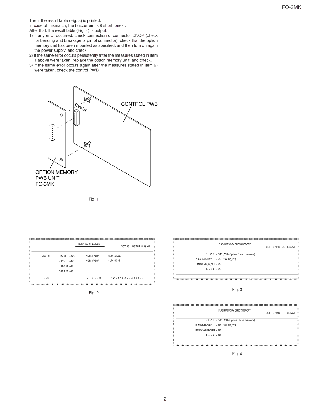
1)If any error occurred, check connection of connector CNOP (check for bending and breakage of pin of connector), check that the option memory unit has been mounted as specified, and then turn on again the power supply, and check.
2)If the same error occurs persistently after the measures stated in item 1 above were taken, replace the option memory unit, and check.
3)If the same error occurs again after the measures stated in item 2) were taken, check the control PWB.
CONTROL PWB
OPTION MEMORY
PWB UNIT
FO-3MK
Fig. 1
ROM/RAM CHECK LIST
|
|
|
| |
|
|
|
| |
|
|
|
|
|
M A I N : | R O M | = OK | VER.=FAB0X | SUM =DE0E |
| C P U | = OK | VER.=FAB0A | SUM =1C86 |
| S R A M | = OK |
|
|
| D R A M = OK |
|
| |
|
|
|
|
|
PCU: |
|
| M / C = 0 0 | F / W = 4 1 2 2 5 0 G 0 0 1 J 0 |
Fig. 2
FLASH MEMORY CHECK REPORT
S I Z E = 5MB (With Option Flash memory)
FLASH MEMORY = OK (15S, 24S, 27S)
BANK CHANGEOVER = OK
B A N K = OK
Fig. 3
FLASH MEMORY CHECK REPORT
S I Z E = 5MB (With Option Flash memory)
FLASH MEMORY = NG (15S, 24S, 27S)
BANK CHANGEOVER = NG
B A N K = NG
Fig. 4
– 2 –