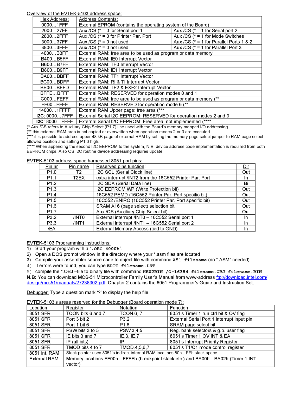
Overview of the
Hex Address: | Address Contents: |
|
0000…1FFF | External EPROM (contains the operating system of the Board) | |
2000…27FF | Aux /CS (* = 0 for Serial port 1 | Aux /CS (* = 1 for Serial port 2 |
2800…2FFF | Aux /CS (* = 0 for Printer Par. Port | Aux /CS (* = 1 for Mode Switches |
3000…37FF | Aux /CS (* = 0 not used | Aux /CS (* = 1 for Parallel Ports 1 & 2 |
3800…3FFF | Aux /CS (* = 0 not used | Aux /CS (* = 1 for Parallel Port 3 |
4000…B3FF | External RAM: free area to be used as program or data memory | |
B400…B5FF | External RAM: IE0 Interrupt Vector |
|
B600…B7FF | External RAM: TF0 Interrupt Vector |
|
B800…B9FF | External RAM: IE1 Interrupt Vector |
|
BA00…BBFF | External RAM: TF1 Interrupt Vector |
|
BC00…BDFF | External RAM: RI & TI Interrupt Vector |
|
BE00…BFFD | External RAM: TF2 & EXF2 Interrupt Vector |
|
BFFE…BFFF | External RAM: RESERVED for operation modes 0 and 1 | |
C000…FEFF | External RAM: free area to be used as program or data memory (** | |
FF00...FFFF | External RAM: RESERVED for operation mode 6 (** | |
14000…1FFFF | External RAM Upper page: free area (*** |
|
I2C: 0000…7FFF | External Serial I2C EEPROM: RESERVED for operation modes 2 and 3 | |
I2C: 8000…FFFF | External Serial I2C EEPROM: Free area, not implemented (**** | |
(* Aux /CS refers to Auxiliary Chip Select (P1.7) line used with the Board’s memory mapped I/O addressing. (** this external RAM area is not copied or overwritten when operation modes 2 or 3 are executed
(*** it is possible to address upper 48 kB page of external RAM by setting the memory page select jumper to RAM page select allowed position and setting P1.6 high.
(**** When appending the second I2C EEPROM to the system, N.B. device address code implementation is required from both EEPROM chips. Also OS I2C routine device addressing requires update.
Pin nr | Pin name | Reserved pins function: | Dir |
P1.0 | T2 | I2C SCL (Serial Clock line) | Out |
P1.1 | T2EX | extra interrupt /INT2 from the 16C552 Printer Par. Port | In |
P1.2 |
| I2C SDA (Serial Data line) | Bi |
P1.3 |
| I2C EEPROM WP (Write Protection bit) | Out |
P1.4 |
| 16C552 PEMD (16C552 Printer Par. Port specific bit) | Out |
P1.5 |
| 16C552 /ENIRQ (16C552 Printer Par. Port specific bit) | Out |
P1.6 |
| SRAM A16 (page select) selection bit | Out |
P1.7 |
| Aux /CS (Auxiliary Chip Select bit) | Out |
P3.2 | /INT0 | External interrupt /INT0 – 16C552 Serial port 1 | In |
P3.3 | /INT1 | External interrupt /INT1 – 16C552 Serial port 2 | In |
/EA |
| External Memory Access (tied to GND) | In |
1)Start your program with a “.ORG 4000h”.
2)Open a DOS prompt window in the directory where your *.asm files are located
3)Compile your assembler source code to object file with command A51 filename (no “.ASM” needed)
4)If errors were found, you can type EDIT filename.LST
5)compile the *.OBJ
Debugger: Type a question mark ‘?’ to display the help file.
Location: | Register | Notation | Function |
8051 SFR | TCON bits 6 and 7 | TCON.6, 7 | 8051’s Timer 1 run ctrl bit & OV flag |
8051 SFR | Port 3 bit 2 | P3.2 | External Serial Port 1 interrupt input pin |
8051 SFR | Port 1 bit 6 | P1.6 | SRAM page select bit |
8051 SFR | PSW bits 3 to 5 | PSW.3,4,5 | Reg. bank selectors & g.p. user flag |
8051 SFR | IE bits 3 and 7 | IE.3, IE.7 | 8051’s Timer 1 OV INT & EA |
8051 SFR | IP (all bits) | IP | 8051’s Interrupt Priority Register |
8051 SFR | TMOD bits 4 to 7 | TMOD.4,5,6,7 | 8051’s T1/C1 mode control register |
8051 int. RAM | Stack pointer uses 8051’s | indirect internal RAM locations 80h…FFh stack space | |
External RAM | Memory locations FF00h…FFFFh (breakpoint stack etc.) and BA00h…BA02h (Timer 1 INT | ||
| vector) |
|
|
