SECTION 6

DIAGRAMS

6.1 Block Diagram - Radio Frequency (RF)


Rx frontend filter


Rx interstage filter


DCS

LNA


1st Rx mixer

IF


IQ Demodulator


RF

IF

SAW Filter


Ceramic Filter


SAW Filter


440 MHz


IF Amplifier (PGC)


I


LO


BB amplifier and


1805..1880 MHz


1805..1880 MHz


90°


0


low pass filter


GSM

LNA


°


Q


RF

IF

RX:


SAW Filter


SAW Filter


GSM 1365..1400 MHz


LO

DCS 1365..1440 MHz


925..960 MHz


925..960 MHz


440 MHz


RX


LO1 (RF) PLL:


Antenna


1


- RX -


GSM 1365..1400 MHz


LNA Bias

Transceiver


2


DCS 1365..1440 MHz


- TX -


control


MHz


Antenna


GSM 1370..1440 MHz


880


DCS 1385..1460 MHz


Switch


TX:


RF Connector with


GSM 1370..1440 MHz


mechanical switch


DCS 1385..1460 MHz


TX


LO2 (IF) PLL


RX 880 MHz


Detector and


TX 975 MHz


2


APC loop

Level control


DCS


GSM


1


MHz


5


TX:


1


GSM

Pin diode

Tx GSM VCO


GSM 685..720 MHz

975


880..915 MHz

switch

880..915 MHz


DCS 1385..1460 MHz


3/5

GSM :5


1

DCS :3


Directional

PA

LP Filter


coupler + LPF


Down


LP Filter


Converter


DCS1800

Pin diode

Tx DCS VCO


1710..1785 MHz

switch

1710..1785 MHz


Sum loop


Loop


Filter

ϕ


I


Directional

PA

LP Filter


90°

0


coupler


Phase


°


detector


GSM 195 MHz


Q


DCS 325 MHz


IC 1

Digital

DET_EN

TX_SW_EN

GSM_TX_EN

GSM_VCO_EN


RF_IC_EN

DET_TX


signals

TXP_OFS_EN

APC_DOWN

DCS_TX_EN

DCS_VCO_EN


IC 2

Analog

AUX_DAC

TXP


signals


VCC_RF LDO

RF_EN

VCC_SYNTH LDO

RXIP

RXIN

RXQP

RXQN

VCTCXO

AFC


13 MHz

CLK13M

NLO1 (RF) PLL


N+1

200 kHz step

Total VCO Range:


1


1365 to 1460 MHz


ϕ


N


1

LO1

Loop


VCO

Filter


PLL


ϕ

N


1

LO2

Loop


VCO

Filter

M

LO2 (IF) PLL


Total VCO Range:

1

1 MHz step


880 to 975 MHz


SERCK

SERDA

SERLE1

SERLE2

TXIP

TXIN

TXQP

TXQN

6.1.1 General RF Indications

The radio part of the CMD-J5/J16 handles the air interface according to the GSM specifications. It is the main contributor for the dualband functionality for E-GSM 900 and DCS 1800.

Receiver

The receiver consists of two separated RF paths for GSM and DCS 1800 each.

On the transmission line between the antenna switch of the RF part and the antenna there is the RF connector including a mechanical switch to connect an external antenna for accessory use. The integrated mechanical switch switches between the helix antenna and the external RF antenna connection. As long as a plug is connected the antenna is deactivated and all RF signals go across the connector.

The GMSK (Gaussian-filtered minimum shift keying) modulated 900 MHz / 1800 MHz signal received by the antenna is filtered, gained and downconverted into the baseband via an intermediate frequency of 440 MHz.

The 440 MHz filter is followed by a tuneable amplifier and IQ demodulator. Behind the demodulator there are additional base band amplifiers and low pass filters.

The In Phase (I) and Quadrature (Q) signal outputs are balanced each.

A13 MHz voltage-controlled-temperature-compensated crystal oscillator (VCTCXO) generates the clock frequency for the PLL and baseband part.

Transmitter

In the transmit direction the digitally GMSK-modulated baseband signal is upconverted to the transmit frequency in the 900 MHz / 1800 MHz band via an intermediate frequency of 195 MHz (GSM) / 325 MHz (DCS 1800) by means of an IQ modulator and the subsequenting sum loop.

All RF and IQ signals are balanced signals in order to suppress crosstalk effects. According to GSM recommendations transmitter and receiver are never active at the same time.

(TDMA system “Time Division Multiple Access”).

17

Page 17
Image 17
Sony CMD-J16 specifications Section Diagrams, Block Diagram Radio Frequency RF, General RF Indications, Transmitter

CMD-J16 specifications

The Sony CMD-J16, released in the late 1990s, exemplifies the innovative spirit of mobile communication technology during that era. This compact mobile phone showcased advanced features for its time, appealing to tech enthusiasts and casual users alike.

One of the standout characteristics of the CMD-J16 is its sleek design. Weighing in at just 113 grams and measuring 135 x 52 x 21 mm, this phone was incredibly portable. The device sported a monochrome display, which supported a resolution of 101 x 32 pixels, offering a simple yet functional interface for users to navigate. Its intuitive button layout made dialing and text input a straightforward process.

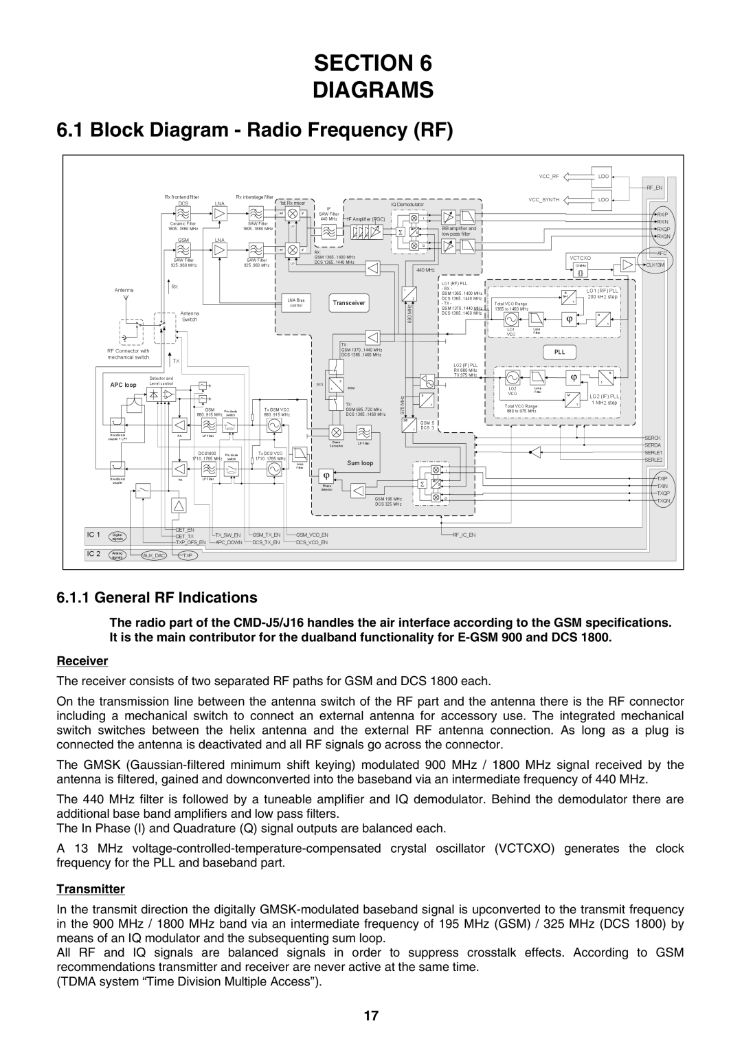
In terms of connectivity, the CMD-J16 operated on GSM technology, which was becoming increasingly popular worldwide. This allowed users to enjoy reliable voice calls and text messaging services. The device supported dual-band GSM, which provided increased coverage and versatility for international travelers.

The phone was equipped with several features that made it user-friendly. One such feature was the integrated phonebook, capable of storing up to 250 contacts. Each contact could hold multiple phone numbers and even a fax number, making it easy for users to manage their communication needs. The CMD-J16 also supported SMS messaging, allowing users to send and receive text messages seamlessly.

Another notable aspect of the CMD-J16 is its long-lasting battery life. The phone housed a NiMH battery, which offered up to 100 hours of standby time and up to 4 hours of talk time, ensuring users could stay connected for extended periods without frequent recharging.

The phone also came with a range of personalization options. Users could select from various ringtones, including polyphonic options, to customize their experience. The device allowed for basic games, adding a touch of entertainment during idle moments.

In summary, the Sony CMD-J16 was a remarkable mobile phone that combined practicality with style. Its compact design, user-friendly features, and reliable performance made it a popular choice among consumers in the late 90s. While it may now be considered a relic in the rapidly evolving world of mobile technology, the CMD-J16 remains a testament to Sony’s commitment to innovation and quality in the telecommunications landscape.