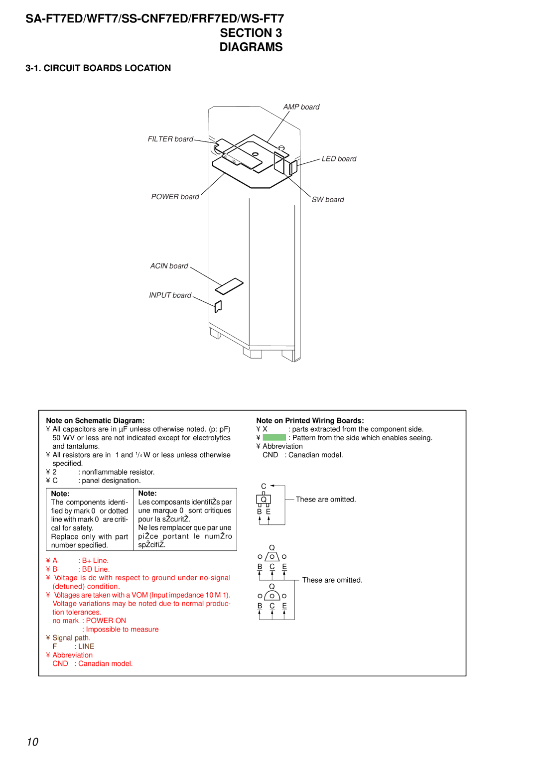
SA-WFT7, SS-FRF7ED specifications
The Sony SS-FRF7ED and SA-WFT7 speaker system represents a harmonious blend of cutting-edge technology and superior audio performance, designed to elevate your listening experience. The SS-FRF7ED is a part of Sony's renowned line of floorstanding speakers, offering a powerful combination of elegance and robust sound. With a sleek design, the SS-FRF7ED can seamlessly integrate into any home environment while delivering stunning acoustic clarity.One of the standout features of the SS-FRF7ED is its three-way configuration, which includes a high-frequency tweeter, mid-range driver, and dual bass drivers. This arrangement ensures that a wide frequency range is covered, allowing for rich highs, clear mids, and powerful lows. The frequency response is impressive, providing a listening experience that caters to various music genres, whether it be classical, rock, or electronic.
The speaker uses Sony's advanced Magnetic Fluid technology, which enhances the overall sound quality by reducing distortion and improving response times. This technology allows for greater dynamic range and ensures that even the most subtle nuances in music are accurately reproduced. The SS-FRF7ED also utilizes optimized bass reflex design, enabling deeper bass performance while minimizing air turbulence, resulting in clean and punchy bass response.
Complementing the SS-FRF7ED is the SA-WFT7 subwoofer, specifically engineered to provide deep, immersive bass that enhances any audio experience. The SA-WFT7 features a high-efficiency amplifier that delivers powerful output without compromising clarity. Its front-firing design and large diameter cone ensure that low frequencies are reproduced with full-bodied detail, making it an ideal partner for movie soundtracks and music alike.
Both the SS-FRF7ED and SA-WFT7 are designed with user convenience in mind. They come equipped with speaker terminals that facilitate easy integration with various audio systems, allowing users to create a comprehensive home theater setup. These speakers also feature a stylish finish that not only enhances their aesthetic appeal but also protects against dust and scratches.
In summary, the Sony SS-FRF7ED and SA-WFT7 speaker combination is an excellent choice for anyone looking to enhance their audio setup with high-quality sound and innovative technology. Whether you’re watching movies, listening to music, or playing video games, the superior performance and advanced features of this speaker system promise to deliver a captivating auditory experience.

