Manuals
/
Sony
/
Home Audio
/
Stereo Amplifier
Sony
Section Electrical Adjustments, TA-E1 SECTION DIAGRAMS, Balance Output Level Adjustment
Models:
TA-E1
1
5
18
18
Download
18 pages
43.31 Kb
1
2
3
4
5
6
7
8
Page 5
Image 5
Page 4
Page 6
Page 5
Image 5
Page 4
Page 6
Contents
SERVICE MANUAL
SPECIFICATIONS
TA-E1
STEREO PRE AMPLIFIER
3. DIAGRAMS
TABLE OF CONTENTS
SAFETY CHECK-OUT
4. EXPLODED VIEWS
SECTION 1 GENERAL
Page
TA-E1 SECTION DIAGRAMS
SECTION ELECTRICAL ADJUSTMENTS
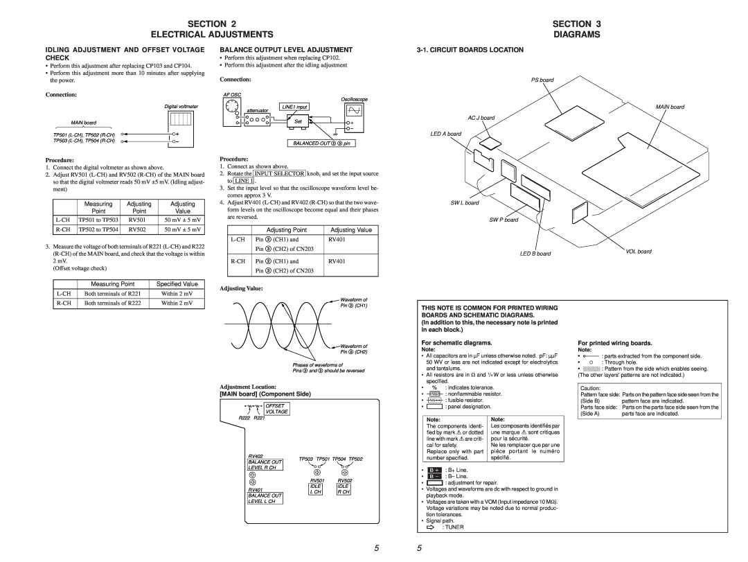
IDLING ADJUSTMENT AND OFFSET VOLTAGE CHECK
BALANCE OUTPUT LEVEL ADJUSTMENT
Refer to page 9 for Printed Wiring Board
3-2. SCHEMATIC DIAGRAM - MAIN SECTION 1/3
TA-E1
Page
Page Page
3-3. SCHEMATIC DIAGRAM - MAIN SECTION 2/3
Page 6 Page
3-4. SCHEMATIC DIAGRAM - MAIN SECTION 3/3
Semiconductor Location
3-5. PRINTED WIRING BOARD - MAIN SECTION
Refer to page 5 for Circuit Boards Location
3-6. SCHEMATIC DIAGRAM - POWER SECTION
Page
3-7. PRINTED WIRING BOARD - POWER SECTION
4-1. TOP PLATE AND BACK PANEL SECTION
SECTION EXPLODED VIEWS
4-2. FRONT PANEL SECTION
not supplied
113
4-3. BOTTOM PLATE SECTION
113 101
Replace only with part number specified
AC J LED A LED B MAIN
SECTION ELECTRICAL PARTS LIST
MAIN
Les composants identifiés par une
for safety
or dotted line with mark !are critical
Ne les remplacer que par une piéce
MAIN
SW L
TA-E1 PS
SW P
9-928-912-11
Top
Page
Image
Contents