
ADS8402 EVM, ADS8412 EVM, ADS8402 specifications
Texas Instruments is renowned for its innovative semiconductor solutions, and the ADS8402 and ADS8412 analog-to-digital converters (ADCs) showcase the company's commitment to precision in data acquisition applications. The ADS8402 is a 16-bit, 2-channel ADC renowned for its high performance and versatility. It operates at data rates up to 1 MSPS (Mega Samples Per Second), making it ideal for a range of applications including industrial automation, high-speed data acquisition systems, and medical instrumentation.The ADS8402 boasts a differential input architecture that enhances noise immunity and improves measurement accuracy. With features such as integrated voltage reference and a programmable gain amplifier, the device allows for adaptability in handling various signal levels. Its low power consumption further extends its appeal for portable and battery-operated devices. The device comes equipped with an internal clock generator, simplifying system design by reducing external components.
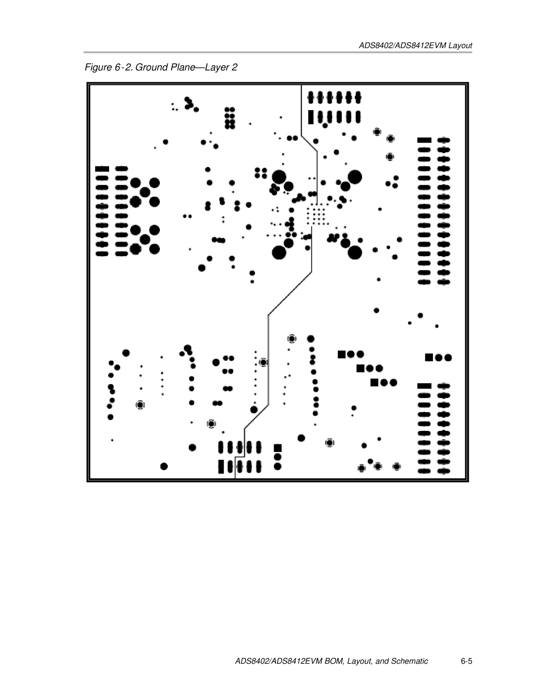
For developers looking to evaluate the performance of the ADS8402, the ADS8402 EVM (Evaluation Module) provides a robust platform. The EVM includes the necessary hardware for quick and convenient testing of the device's capabilities. It features numerous connectivity options, enabling users to interface with a variety of microcontrollers and processors. Benefiting from TI's extensive software support, the EVM allows for easy data visualization and manipulation through compatible software platforms.
On the other hand, the ADS8412 is an advanced 16-bit ADC with a single channel and supports faster sampling rates up to 2 MSPS. It is designed for applications requiring high precision and high throughput. The device features an integrated digital filter that significantly lowers noise and enhances signal integrity. The ADS8412 is particularly well-suited for precision measurement systems in industries such as telecommunications and data acquisition.
The ADS8412 EVM caters to users who wish to explore the capabilities of the ADS8412 with ease. Similar to the ADS8402 EVM, the ADS8412 evaluation module provides structured support for testing with readily available interfaces. This makes it an invaluable tool for engineers and developers looking to integrate high-performance ADCs into their designs.
Both the ADS8402 and ADS8412 ADCs exemplify Texas Instruments' dedication to delivering high-quality, innovative technologies that meet the demands of modern applications. With their combination of precision, speed, and adaptability, these ADCs are excellent choices for engineers seeking reliable data acquisition solutions.