Texas Instruments TPS650231EVM, TPS65023B manual Evaluation Board/Kit Important Notice, FCC Warning

Models: TPS65023B TPS650231EVM

1 14
Download 14 pages 25.48 Kb
Page 13
Image 13

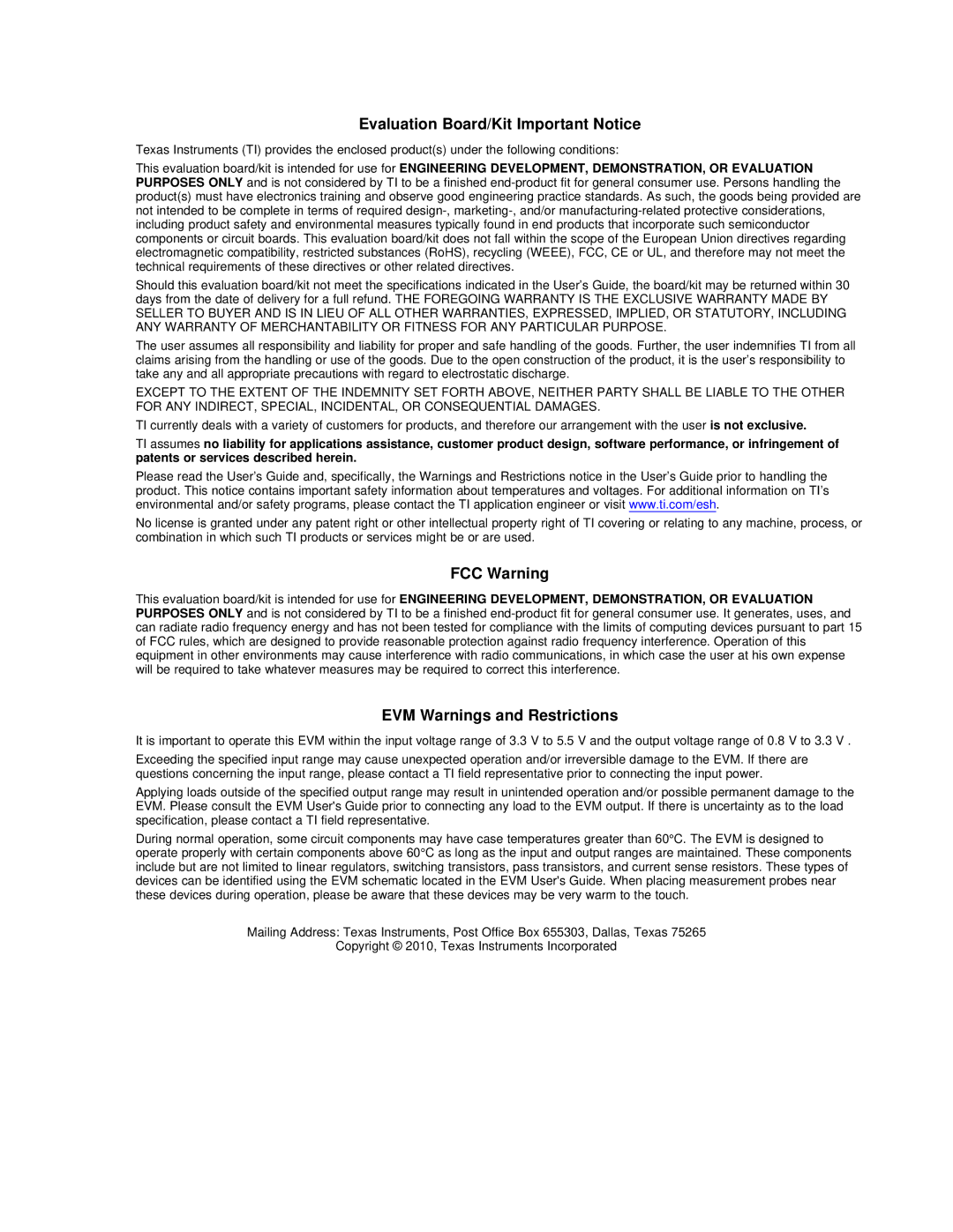
Evaluation Board/Kit Important Notice

Texas Instruments (TI) provides the enclosed product(s) under the following conditions:

This evaluation board/kit is intended for use for ENGINEERING DEVELOPMENT, DEMONSTRATION, OR EVALUATION PURPOSES ONLY and is not considered by TI to be a finished end-product fit for general consumer use. Persons handling the product(s) must have electronics training and observe good engineering practice standards. As such, the goods being provided are not intended to be complete in terms of required design-,marketing-, and/or manufacturing-related protective considerations, including product safety and environmental measures typically found in end products that incorporate such semiconductor components or circuit boards. This evaluation board/kit does not fall within the scope of the European Union directives regarding electromagnetic compatibility, restricted substances (RoHS), recycling (WEEE), FCC, CE or UL, and therefore may not meet the technical requirements of these directives or other related directives.

Should this evaluation board/kit not meet the specifications indicated in the User’s Guide, the board/kit may be returned within 30 days from the date of delivery for a full refund. THE FOREGOING WARRANTY IS THE EXCLUSIVE WARRANTY MADE BY SELLER TO BUYER AND IS IN LIEU OF ALL OTHER WARRANTIES, EXPRESSED, IMPLIED, OR STATUTORY, INCLUDING ANY WARRANTY OF MERCHANTABILITY OR FITNESS FOR ANY PARTICULAR PURPOSE.

The user assumes all responsibility and liability for proper and safe handling of the goods. Further, the user indemnifies TI from all claims arising from the handling or use of the goods. Due to the open construction of the product, it is the user’s responsibility to take any and all appropriate precautions with regard to electrostatic discharge.

EXCEPT TO THE EXTENT OF THE INDEMNITY SET FORTH ABOVE, NEITHER PARTY SHALL BE LIABLE TO THE OTHER FOR ANY INDIRECT, SPECIAL, INCIDENTAL, OR CONSEQUENTIAL DAMAGES.

TI currently deals with a variety of customers for products, and therefore our arrangement with the user is not exclusive.

TI assumes no liability for applications assistance, customer product design, software performance, or infringement of patents or services described herein.

Please read the User’s Guide and, specifically, the Warnings and Restrictions notice in the User’s Guide prior to handling the product. This notice contains important safety information about temperatures and voltages. For additional information on TI’s environmental and/or safety programs, please contact the TI application engineer or visit www.ti.com/esh.

No license is granted under any patent right or other intellectual property right of TI covering or relating to any machine, process, or combination in which such TI products or services might be or are used.

FCC Warning

This evaluation board/kit is intended for use for ENGINEERING DEVELOPMENT, DEMONSTRATION, OR EVALUATION PURPOSES ONLY and is not considered by TI to be a finished end-product fit for general consumer use. It generates, uses, and can radiate radio frequency energy and has not been tested for compliance with the limits of computing devices pursuant to part 15 of FCC rules, which are designed to provide reasonable protection against radio frequency interference. Operation of this equipment in other environments may cause interference with radio communications, in which case the user at his own expense will be required to take whatever measures may be required to correct this interference.

EVM Warnings and Restrictions

It is important to operate this EVM within the input voltage range of 3.3 V to 5.5 V and the output voltage range of 0.8 V to 3.3 V .

Exceeding the specified input range may cause unexpected operation and/or irreversible damage to the EVM. If there are questions concerning the input range, please contact a TI field representative prior to connecting the input power.

Applying loads outside of the specified output range may result in unintended operation and/or possible permanent damage to the EVM. Please consult the EVM User's Guide prior to connecting any load to the EVM output. If there is uncertainty as to the load specification, please contact a TI field representative.

During normal operation, some circuit components may have case temperatures greater than 60°C. The EVM is designed to operate properly with certain components above 60°C as long as the input and output ranges are maintained. These components include but are not limited to linear regulators, switching transistors, pass transistors, and current sense resistors. These types of devices can be identified using the EVM schematic located in the EVM User's Guide. When placing measurement probes near these devices during operation, please be aware that these devices may be very warm to the touch.

Mailing Address: Texas Instruments, Post Office Box 655303, Dallas, Texas 75265

Copyright © 2010, Texas Instruments Incorporated

Page 13
Image 13
Texas Instruments TPS650231EVM manual Evaluation Board/Kit Important Notice, FCC Warning, EVM Warnings and Restrictions

TPS65023B, TPS650231EVM specifications

Texas Instruments has a reputation for producing high-quality power management solutions, and the TPS650231EVM and TPS65023B are perfect examples of this. These advanced power management modules are designed for efficient power delivery in various applications, including portable devices and embedded systems.

The TPS650231EVM is an evaluation module developed to facilitate the evaluation of the TPS65023B power management IC. This device is specifically engineered to deliver power to processors that require multiple outputs from a single power source. The TPS65023B integrates several key features that make it a robust choice for designers aiming to simplify their power management requirements.

One of the main highlights of the TPS65023B is its dual buck converter. This converter can efficiently convert the input voltage into multiple output voltages, specifically optimized for powering processors and other system components. The device supports adjustable output voltages, allowing developers to tune the system to meet the exact power needs of their applications. With an input voltage range of 2.5V to 5.5V, the TPS65023B can accommodate diverse power input requirements.

Another key technology incorporated in the TPS65023B is the ultra-low quiescent current specification, which helps extend battery life in portable applications. This is particularly important in battery-powered devices, where optimization of power consumption is critical. The device also incorporates various protection features, including thermal shutdown, over-voltage protection, and short-circuit protection, ensuring reliable operation under various conditions.

The TPS65023B features a small footprint, making it ideal for space-constrained designs. The integration of multiple power management functions into a single device not only saves board space but also simplifies the design process, allowing engineers to focus on other critical aspects of their applications.

In addition to its technical specifications, the TPS650231EVM provides a user-friendly platform for evaluating the performance of the TPS65023B. This evaluation module includes necessary components and design considerations, enabling developers to quickly assess the device's capabilities within their systems.

In summary, the Texas Instruments TPS650231EVM and TPS65023B offer cutting-edge features, advanced technology, and robust performance. Their versatility and efficiency make them highly suitable for a range of applications, helping engineers achieve their design goals while maximizing power efficiency and reliability.