| 4/8GB microSDHC Class 6 Card + Reader P3 | |
|
|
|
•Bus Signal Levels
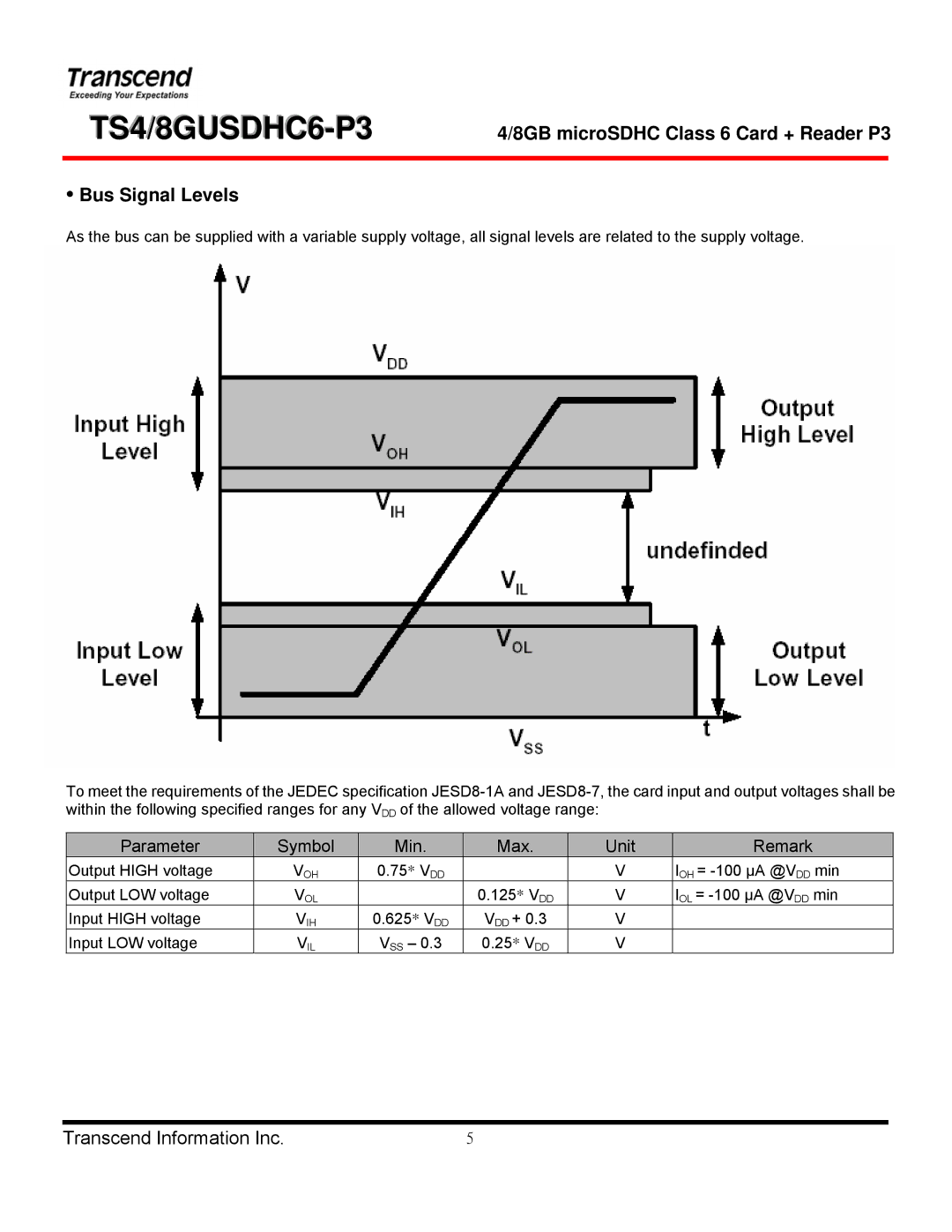
As the bus can be supplied with a variable supply voltage, all signal levels are related to the supply voltage.
To meet the requirements of the JEDEC specification
Parameter | Symbol | Min. | Max. | Unit | Remark |
Output HIGH voltage | VOH | 0.75* VDD |
| V | IOH = |
Output LOW voltage | VOL |
| 0.125* VDD | V | IOL = |
Input HIGH voltage | VIH | 0.625* VDD | VDD + 0.3 | V |
|
Input LOW voltage | VIL | VSS – 0.3 | 0.25* VDD | V |
|
Transcend Information Inc. | 5 |
