CTX2500 Card Description
The CTX2500 card provides 576 x 576
The CTX2500 card can be installed in Slot 3 or 4. Protection switches between the active and standby CTX 2500 are hitless (less than a
The CTX2500 supports errorless side switches (switching from one CTX2500 on one side of the shelf to the other CTX2500 on the other side of the shelf) when the switch is initiated through software or is caused by a software upgrade.
There are two PPM (SFP) slots on the CTX2500 faceplate. Each slot can contain a
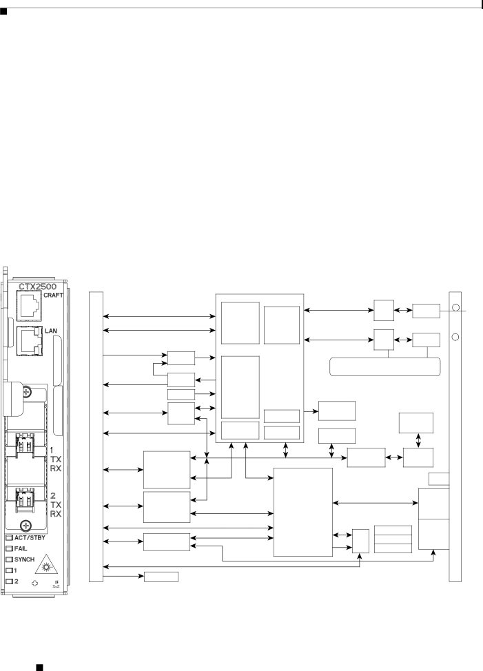
Faceplate and Block Diagram
Figure 1 shows the CTX2500 card faceplate and block diagram.
Figure 1 | CTX2500 Faceplate and Block Diagram |
|
|
| STS1 XC |
|
| XPT |
|
|
| SFP1 |
|
|
|
|
| SW |
|
|
| ||
|
|
|
|
|
|
|
|
| ||
|
|
| TU XC | OCN I/F |
|
|
|
|
|
|
|
|
| VT XC |
|
| XPT |
|
|
| SFP1 |
|
|
|
|
|
| SW |
|
|
| |
| REFCLK_IN |
|
|
|
|
|
|
|
| |
| PLL |
|
|
|
|
|
|
|
| |
|
|
|
| XPT and SFP Control/Status | ||||||
|
|
|
|
| ||||||
|
| VXCO |
| ASIC | From Nile2 CPLD | |||||
|
| TIMING |
|
|
|
|
|
| ||
| REFCLK_OUT |
|
|
|
|
|
|
|
| |
Connectors | OCXO | MOD | CPU I/F | FLASH |
|
|
|
|
| |
|
|
|
|
|
|
|
| |||
|
| LIU |
|
| Compact |
|
|
|
|
|
|
|
| ATA I/F | FLASH |
|
|
| DDR | ||
|
|
|
|
|
|
| ||||
|
|
| SCL I/F |
|
|
| SDRAM | |||
Backplane |
|
|
|
|
|
|
|
|
| |
|
|
|
| BUS |
|
| FPGA | |||
|
|
|
|
|
|
| ||||
|
|
|
|
| FANOUT |
| ||||
| FPGA |
|
|
|
|
|
| |||
|
|
|
|
|
|
|
| LED | ||
|
|
|
|
|
|
|
|
|
| |
|
|
|
|
|
|
|
|
|
| RJ45 |
| CPLD |
| PROCESSOR |
|
|
|
| FP | ||
|
|
|
|
|
| CRAFT | ||||
|
|
|
|
|
|
|
| |||
|
|
|
|
|
| TEMP |
|
| RJ45 | |
|
|
|
|
| I2C |
|
| FP | ||
| ENWT SW |
|
| SFP1/2 |
| |||||
|
|
|
| ENET | ||||||
|
|
|
| IDPROM | ||||||
|
|
|
|
|
|
| ||||
| DC/DC |
|
|
|
|
|
|
|
| |
Front Panel
145768
Installing the CTX2500 Card in the Cisco ONS
2 |
| |
|