CY7C1231H
Switching Waveforms (continued)
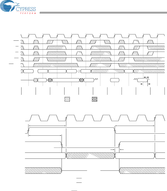
NOP, STALL and Deselect Cycles[18, 19, 21]
CLK
CEN
CE
ADV/LD
WE
BW[A:B]
ADDRESS
DQ
COMMAND
1 | 2 | 3 | 4 | 5 |
A1 ![]() A2
A2 ![]() A3
A3 ![]() A4
A4
| D(A1) |
| Q(A2) | Q(A3) |
WRITE | READ | STALL | READ | WRITE |
D(A1) | Q(A2) |
| Q(A3) | D(A4) |
6 | 7 | 8 | 9 | 10 |
A5
tCHZ
![]()
![]() D(A4)
D(A4) ![]()
![]() Q(A5)
Q(A5) ![]()
|
|
| tDOH |
STALL | NOP | READ | DESELECT CONTINUE |
|
| Q(A5) | DESELECT |
DON’T CARE | UNDEFINED |
ZZ Mode Timing[22, 23]
CLK
ZZ
ISUPPLY
ALL INPUTS (except ZZ)
Outputs (Q)
tZZ
t ZZI
I DDZZ

 DON’T CARE
t ZZREC
t RZZI
DESELECT or READ Only
Notes:
21.The IGNORE CLOCK EDGE or STALL cycle (Clock 3) illustrated CEN being used to create a pause. A write is not performed during this cycle.
22.Device must be deselected when entering ZZ mode. See Truth Table for all possible signal conditions to deselect the device.
23.I/Os are in
Document #: | Page 10 of 12 |
[+] Feedback