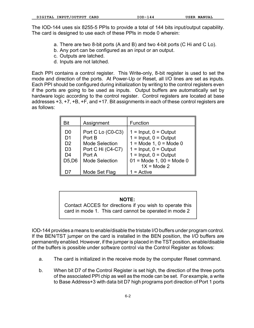
IOD-144 specifications
Access IOD-144 is a cutting-edge device that has garnered significant attention within the field of connectivity solutions. Designed primarily for industrial applications, the IOD-144 is an Internet of Things (IoT) gateway that facilitates seamless communication between devices and applications in a robust and reliable manner. This device is particularly suited for environments that require real-time data processing and monitoring, making it an ideal choice for sectors like manufacturing, transportation, and smart cities.One of the standout features of the Access IOD-144 is its versatility in supporting multiple connectivity options. It is equipped to handle various protocols, including Ethernet, Wi-Fi, Bluetooth, and cellular networks. This broad support ensures that users can choose the most suitable connectivity method based on their specific requirements and existing infrastructure. The device's ability to adapt to different network environments enhances its utility in diverse operational settings.
In terms of processing power, the IOD-144 prides itself on having a powerful microprocessor, allowing it to perform complex computations and data processing locally. This edge computing capability reduces latency by enabling real-time data analysis and decision-making without the need to constantly communicate with a cloud service. As a result, businesses benefit from faster response times and reduced bandwidth costs.
Moreover, the Access IOD-144 is designed with scalability in mind. It can support an extensive array of sensors and actuators, making it an ideal solution for organizations looking to expand their IoT ecosystems over time. The device can easily integrate with various third-party applications and platforms, ensuring compatibility and allowing for future growth.
Security is another key focus of the IOD-144. With built-in encryption protocols and secure authentication methods, the device helps to safeguard data transmitted across networks. This emphasis on security is crucial, particularly in industrial settings where data breaches can have severe consequences.
Additional features of the Access IOD-144 include user-friendly management software that simplifies deployment, monitoring, and maintenance of connected devices. The device also supports over-the-air firmware updates, ensuring that users can keep their systems up-to-date with the latest features and security enhancements.
In summary, the Access IOD-144 stands out due to its multifaceted connectivity options, powerful processing capabilities, scalability, robust security measures, and user-friendly management tools. These characteristics make it a leading choice for businesses looking to enhance their IoT capabilities while ensuring reliable performance in challenging environments.

