SPC-57 specifications
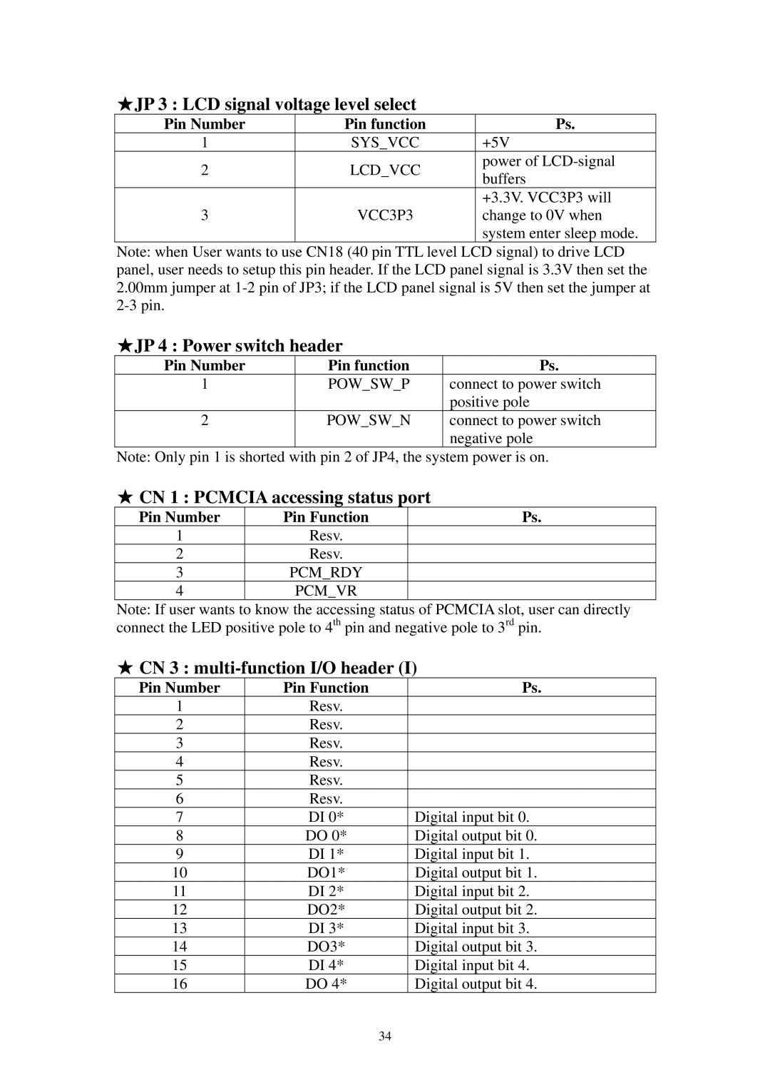
The Advantech SPC-57 is a versatile and robust industrial computer designed for a wide range of applications in demanding environments. This system integrates advanced technologies and features to ensure high performance and reliability, making it ideal for automation, control, and data processing tasks across various industries.One of the standout characteristics of the SPC-57 is its compact form factor. Despite its small size, it is equipped with powerful processing capabilities, utilizing the latest Intel processors to deliver exceptional computing power. This enables users to handle complex tasks efficiently, making it suitable for real-time data acquisition and processing.
The SPC-57 features a modular design that allows for easy customization and expansion. Users can select various I/O modules to tailor the system to their specific needs, whether it involves adding additional communication ports, analog inputs, or other specialized interfaces. This flexibility ensures that the SPC-57 can adapt to changing requirements over time.
Connectivity is another key advantage of the SPC-57. It offers multiple communication options, including Ethernet, serial ports, and USB interfaces. This extensive range of connectivity options makes it easy to integrate the SPC-57 into existing industrial networks, facilitating seamless communication with other devices and systems.
For enhanced reliability, the SPC-57 is built to withstand harsh environmental conditions. It is designed with a wide operating temperature range, shock and vibration resistance, and protection against dust and moisture. This rugged construction ensures that the system can operate effectively in factories, outdoor locations, and other challenging settings.
In terms of power efficiency, the SPC-57 employs advanced power management technologies. This not only reduces energy consumption but also prolongs the system's operational lifespan, making it a cost-effective solution for long-term use in industrial applications.
The user-friendly design of the SPC-57, combined with its robust features, makes it an excellent choice for industries such as manufacturing, transportation, and energy. With its ability to function reliably in various scenarios, the Advantech SPC-57 is a forward-thinking solution that meets the demands of modern industrial automation and control systems.
