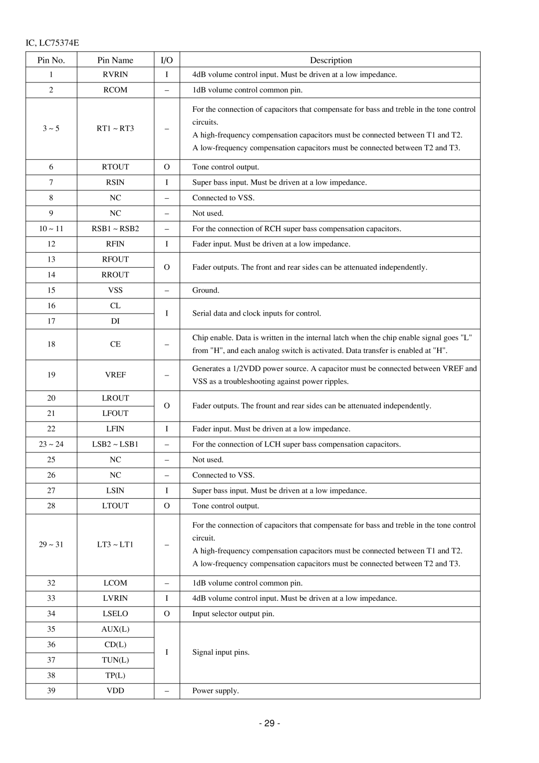
IC, LC75374E
Pin No. | Pin Name | I/O | Description | |
|
|
|
| |
1 | RVRIN | I | 4dB volume control input. Must be driven at a low impedance. | |
|
|
|
| |
2 | RCOM | – | 1dB volume control common pin. | |
|
|
|
| |
|
|
| For the connection of capacitors that compensate for bass and treble in the tone control | |
3 ~ 5 | RT1 ~ RT3 | – | circuits. | |
A | ||||
|
|
| ||
|
|
| A | |
|
|
|
| |
6 | RTOUT | O | Tone control output. | |
|
|
|
| |
7 | RSIN | I | Super bass input. Must be driven at a low impedance. | |
|
|
|
| |
8 | NC | – | Connected to VSS. | |
|
|
|
| |
9 | NC | – | Not used. | |
|
|
|
| |
10 ~ 11 | RSB1 ~ RSB2 | – | For the connection of RCH super bass compensation capacitors. | |
|
|
|
| |
12 | RFIN | I | Fader input. Must be driven at a low impedance. | |
|
|
|
| |
13 | RFOUT | O | Fader outputs. The front and rear sides can be attenuated independently. | |
|
| |||
14 | RROUT | |||
|
| |||
|
|
|
| |
15 | VSS | – | Ground. | |
|
|
|
| |
16 | CL | I | Serial data and clock inputs for control. | |
|
| |||
17 | DI | |||
|
| |||
|
|
|
| |
18 | CE | – | Chip enable. Data is written in the internal latch when the chip enable signal goes "L" | |
from "H", and each analog switch is activated. Data transfer is enabled at "H". | ||||
|
|
| ||
|
|
|
| |
19 | VREF | – | Generates a 1/2VDD power source. A capacitor must be connected between VREF and | |
VSS as a troubleshooting against power ripples. | ||||
|
|
| ||
|
|
|
| |
20 | LROUT | O | Fader outputs. The frount and rear sides can be attenuated independently. | |
|
| |||
21 | LFOUT | |||
|
| |||
|
|
|
| |
22 | LFIN | I | Fader input. Must be driven at a low impedance. | |
|
|
|
| |
23 ~ 24 | LSB2 ~ LSB1 | – | For the connection of LCH super bass compensation capacitors. | |
|
|
|
| |
25 | NC | – | Not used. | |
|
|
|
| |
26 | NC | – | Connected to VSS. | |
|
|
|
| |
27 | LSIN | I | Super bass input. Must be driven at a low impedance. | |
|
|
|
| |
28 | LTOUT | O | Tone control output. | |
|
|
|
| |
|
|
| For the connection of capacitors that compensate for bass and treble in the tone control | |
29 ~ 31 | LT3 ~ LT1 | – | circuit. | |
A | ||||
|
|
| ||
|
|
| A | |
|
|
|
| |
32 | LCOM | – | 1dB volume control common pin. | |
|
|
|
| |
33 | LVRIN | I | 4dB volume control input. Must be driven at a low impedance. | |
|
|
|
| |
34 | LSELO | O | Input selector output pin. | |
|
|
|
| |
35 | AUX(L) |
|
| |
|
|
|
| |
36 | CD(L) | I | Signal input pins. | |
|
| |||
37 | TUN(L) | |||
|
| |||
|
|
|
| |
38 | TP(L) |
|
| |
|
|
|
| |
39 | VDD | – | Power supply. | |
|
|
|
|
- 29 -
