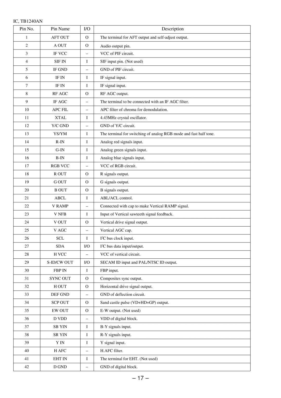
IC, TB1240AN
Pin No. | Pin Name | I/O | Description |
|
|
|
|
1 | AFT OUT | O | The terminal for AFT output and |
|
|
|
|
2 | A OUT | O | Audio output pin. |
|
|
|
|
3 | IF VCC | – | VCC of PIF circuit. |
|
|
|
|
4 | SIF IN | I | SIF input pin. (Not used) |
|
|
|
|
5 | IF GND | – | GND of PIF circuit. |
|
|
|
|
6 | IF IN | I | IF signal input. |
|
|
|
|
7 | IF IN | I | IF signal input. |
|
|
|
|
8 | RF AGC | O | RF AGC output. |
|
|
|
|
9 | IF AGC | – | The terminal to be connected with an IF AGC filter. |
|
|
|
|
10 | APC FIL | – | APC filter of chroma for demodulation. |
|
|
|
|
11 | XTAL | I | 4.43MHz crystal oscillator. |
|
|
|
|
12 | Y/C GND | – | GND of Y/C circuit. |
|
|
|
|
13 | YS/YM | I | The terminal for switching of analog RGB mode and fast half tone. |
|
|
|
|
14 | I | Analog red signals input. | |
|
|
|
|
15 | I | Analog green signals input. | |
|
|
|
|
16 | I | Analog blue signals input. | |
|
|
|
|
17 | RGB VCC | – | VCC of RGB circuit. |
|
|
|
|
18 | R OUT | O | R signals output. |
|
|
|
|
19 | G OUT | O | G signals output. |
|
|
|
|
20 | B OUT | O | B signals output. |
|
|
|
|
21 | ABCL | I | ABL/ACL control. |
|
|
|
|
22 | V RAMP | – | Connected with cap to make Vertical RAMP signal. |
|
|
|
|
23 | V NFB | I | Input of Vertical sawteeth signal feedback. |
|
|
|
|
24 | V OUT | O | Vertical drive signal output. |
|
|
|
|
25 | V AGC | – | Vertical AGC cap. |
|
|
|
|
26 | SCL | I | I2C bus clock input. |
|
|
|
|
27 | SDA | I/O | I2C bus data input/output. |
|
|
|
|
28 | H VCC | – | VCC of vertical circuit. |
|
|
|
|
29 | I/O | SECAM ID input and PAL/NTSC ID output. | |
|
|
|
|
30 | FBP IN | I | FBP input. |
|
|
|
|
31 | SYNC OUT | O | Composites sync output. |
|
|
|
|
32 | H OUT | O | Horizontal drive signal output. |
|
|
|
|
33 | DEF GND | – | GND of deflection circuit. |
|
|
|
|
34 | SCP OUT | O | Sand castle pulse (VD+HD+GP) output. |
|
|
|
|
35 | EW OUT | O | |
|
|
|
|
36 | D VDD | – | VDD of digital block. |
|
|
|
|
37 | SB YIN | I | |
|
|
|
|
38 | SR YIN | I | |
|
|
|
|
39 | Y IN | I | Y signal input. |
|
|
|
|
40 | H AFC | – | H.AFC filter. |
|
|
|
|
41 | EHT IN | I | The terminal for EHT. (Not used) |
|
|
|
|
42 | D GND | – | GND of digital block. |
|
|
|
|
– 17 –