BIG MEMORY BIG MEMORY BIG MEMORY BIG MEMORY BIG MEMORY BIG MEMORY BIG MEMORY BIG MEMORY BIG MEMORY BIG MEMORY BIG MEMORY BIG MEMORY SFR DESCRIPTIONS
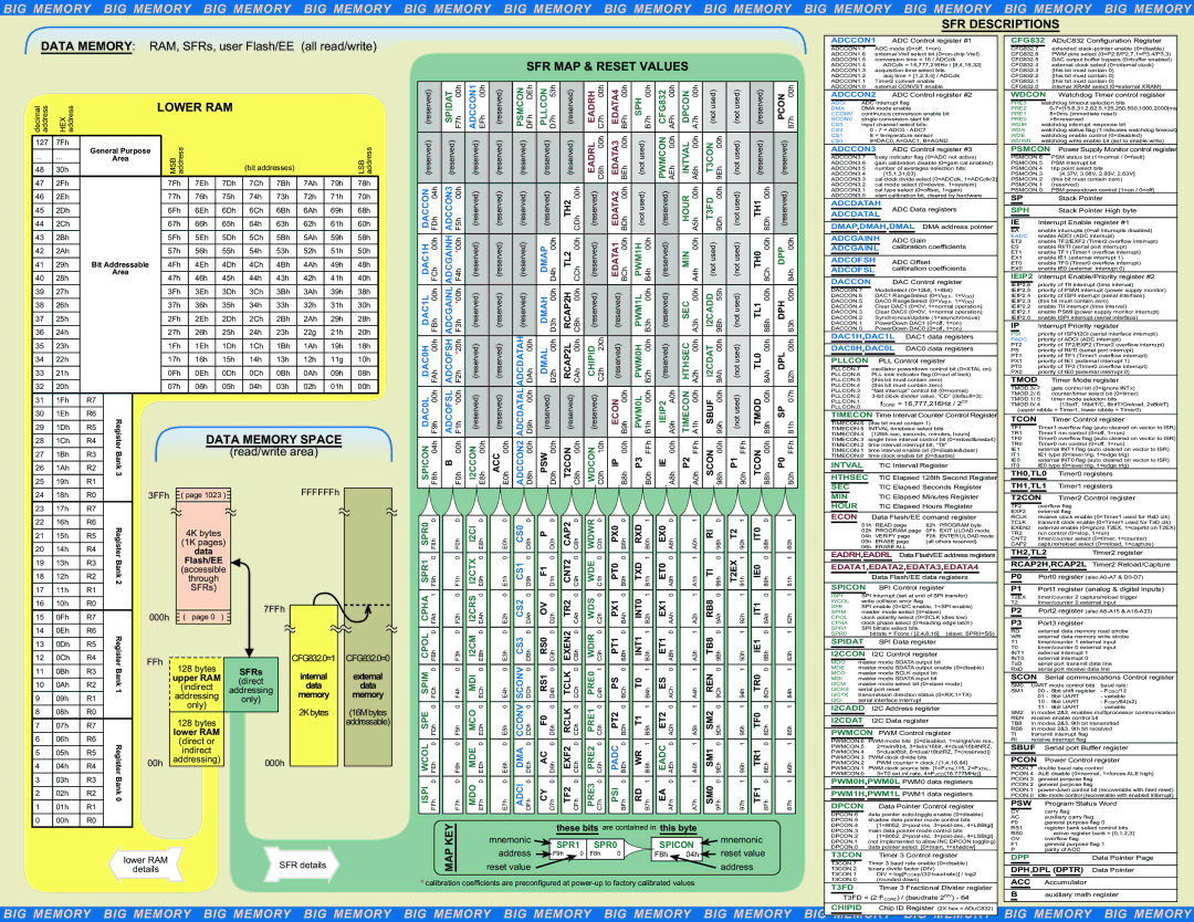
DATA MEMORY: RAM, SFRs, user Flash/EE (all read/write)
SFR MAP & RESET VALUES
| ADCCON1 | ADC Control register #1 |
| ADCCON1.7 | ADC mode (0=off, 1=on) |
| ADCCON1.6 | external Vref select bit |
| ADCCON1.5 | conversion time = 16 / ADCclk |
| ADCCON1.4 | ADCclk = 16,777,216Hz / [8,4,16,32] |
| ADCCON1.3 | acquisition time select bits |
| ADCCON1.2 | acq time = [1,2,3,4] / ADCclk |
| ADCCON1.1 | Timer2 convert enable |
| CFG832 | ADuC832 Configuration Register |
| CFG832.7 | extended |
| CFG832.6 | PWM pins select (0=P2.6/P2.7,1=P3.4/P3.3) |
| CFG832.5 | DAC output buffer bypass (0=buffer enabled) |
| CFG832.4 | external clock select (0=internal clock) |
| CFG832.3 | (this bit must contain 0) |
| CFG832.2 | (this bit must contain 0) |
| CFG832.1 | (this bit must contain 0) |
decimal address | HEX address |
| LOWER RAM |
|
| ||
|
|
|
|
| |||
|
|
|
|
|
|
| |
127 | 7Fh | General Purpose |
| ss |
| LSBaddress | |
|
|
| (bit addresses) | ||||
48 | 30h | ||||||
|
| SBMddrea | |||||
... ... | Area |
|
|
|
| ||
|
|
|
|
|
| ||
|
|
|
|
|
|
| |
47 | 2Fh |
|
|
| 7Fh | 7Eh | 7Dh | 7Ch | 7Bh | 7Ah | 79h | 78h |
46 | 2Eh |
|
|
| 77h | 76h | 75h | 74h | 73h | 72h | 71h | 70h |
45 | 2Dh |
|
|
| 6Fh | 6Eh | 6Dh | 6Ch | 6Bh | 6Ah | 69h | 68h |
44 | 2Ch |
|
|
| 67h | 66h | 65h | 64h | 63h | 62h | 61h | 60h |
43 | 2Bh |
|
|
| 5Fh | 5Eh | 5Dh | 5Ch | 5Bh | 5Ah | 59h | 58h |
42 | 2Ah |
|
|
| 57h | 56h | 55h | 54h | 53h | 52h | 51h | 50h |
41 | 29h | Bit Addressable | 4Fh | 4Eh | 4Dh | 4Ch | 4Bh | 4Ah | 49h | 48h | ||
40 | 28h |
| Area | 47h | 46h | 45h | 44h | 43h | 42h | 41h | 40h | |
|
|
| ||||||||||
39 | 27h |
|
|
| 3Fh | 3Eh | 3Dh | 3Ch | 3Bh | 3Ah | 39h | 38h |
38 | 26h |
|
|
| 37h | 36h | 35h | 34h | 33h | 32h | 31h | 30h |
37 | 25h |
|
|
| 2Fh | 2Eh | 2Dh | 2Ch | 2Bh | 2Ah | 29h | 28h |
36 | 24h |
|
|
| 27h | 26h | 25h | 24h | 23h | 22g | 21h | 20h |
35 | 23h |
|
|
| 1Fh | 1Eh | 1Dh | 1Ch | 1Bh | 1Ah | 19h | 18h |
34 | 22h |
|
|
| 17h | 16h | 15h | 14h | 13h | 12h | 11g | 10h |
33 | 21h |
|
|
| 0Fh | 0Eh | 0Dh | 0Ch | 0Bh | 0Ah | 09h | 08h |
32 | 20h |
|
|
| 07h | 06h | 05h | 04h | 03h | 02h | 01h | 00h |
31 | 1Fh | R7 |
|
|
|
|
|
|
|
|
|
|
30 | 1Eh | R6 | Register |
|
|
|
|
|
|
|
|
|
29 | 1Dh | R5 |
|
|
|
|
|
|
|
|
| |
28 | 1Ch | R4 |
|
| DATA MEMORY SPACE |
| ||||||
27 | 1Bh | R3 |
|
|
| (read/write area) |
|
| ||||
Bank |
|
|
|
|
| |||||||
26 | 1Ah | R2 |
|
|
|
|
|
|
|
|
| |
3 |
|
|
|
|
|
|
|
|
| |||
|
|
|
|
|
|
|
|
|
|
|
| |
25 | 19h | R1 |
|
|
|
|
|
|
|
|
|
|
24 | 18h | R0 |
| 3FFh | ( page 1023 ) |
|
| FFFFFFh |
| |||
|
|
|
|
|
| |||||||
23 | 17h | R7 |
|
|
|
|
|
|
|
|
|
|
22 | 16h | R6 | Register |
|
|
|
|
|
|
|
|
|
21 | 15h | R5 |
|
| 4K bytes |
|
|
|
|
|
| |
20 | 14h | R4 |
|
| (1K pages) |
|
|
|
|
| ||
|
| data |
|
|
|
|
|
| ||||
|
|
|
|
| Flash/EE |
|
|
|
|
| ||
19 | 13h | R3 | Bank2 |
|
|
|
|
|
|
| ||
18 | 12h | R2 |
|
| (accessible |
|
|
|
|
| ||
|
| through |
|
|
|
|
|
| ||||
17 | 11h | R1 |
|
|
| SFRs) |
|
|
|
|
|
|
16 | 10h | R0 |
|
|
|
|
|
| 7FFh |
|
|
|
15 | 0Fh | R7 |
| 000h | ( page 0 | ) |
|
|
|
| ||
|
|
|
|
|
| |||||||
14 | 0Eh | R6 | Register |
|
|
|
|
|
|
|
|
|
13 | 0Dh | R5 |
|
|
|
|
|
|
|
|
| |
12 | 0Ch | R4 | FFh | 128 bytes |
| SFRs |
| CFG832.0=1 | CFG832.0=0 | |||
11 | 0Bh | R3 | Bank 1 |
|
|
| internal |
| external | |||
| upper RAM |
|
|
| ||||||||
|
|
|
|
| (direct |
|
| |||||
10 | 0Ah | R2 |
| (indirect |
|
| data |
| data | |||
| addressing |
| ||||||||||
|
|
|
|
| ||||||||
9 | 09h | R1 |
|
| addressing |
| only) |
| memory |
| memory | |
|
|
| only) |
|
|
|
|
| ||||
8 | 08h | R0 |
|
|
|
|
|
| 2K bytes |
| (16M bytes | |
|
|
|
|
|
|
|
| |||||
7 | 07h | R7 |
|
| 128 bytes |
|
|
|
|
| addressable) | |
6 | 06h | R6 |
|
| lower RAM |
|
|
|
|
|
| |
Register |
| (direct or |
|
|
|
|
|
| ||||
5 | 05h | R5 |
|
| indirect |
|
|
|
|
|
| |
4 | 04h | R4 | 00h | addressing) |
|
| 000h |
|
|
| ||
|
|
|
|
|
|
|
|
| ||||
|
|
|
|
|
|
|
|
|
|
|
| |
3 | 03h | R3 | Bank |
|
|
|
|
|
|
|
|
|
2 | 02h | R2 |
|
|
|
|
|
|
|
|
| |
0 |
|
|
|
|
|
|
|
|
| |||
|
|
|
|
|
|
|
|
|
|
|
| |
1 | 01h | R1 |
|
|
|
|
|
|
|
|
|
|
0 | 00h | R0 |
|
|
|
|
|
|
|
|
|
|
|
|
|
| lower RAM |
|
|
|
| SFR details |
|
| |
|
|
|
| details |
|
|
|
|
|
| ||
|
|
|
|
|
|
|
|
|
|
|
| |
(reserved) | SPIDAT F7h 00h | ADCCON1 EFh 00h | (reserved) | PSMCON DFh DEh | PLLCON D7h 53h | (reserved) | EADRH C7h 00h | EDATA4 BFh 00h | SPH B7h 00h | CFG832 AFh 00h | DPCON A7h 00h | (not used) | (not used) | (reserved) | PCON | 87h 00h | |||||
(reserved) | (reserved) | (reserved) | (reserved) | (reserved) | (reserved) | (reserved) | EADRL C6h 00h | EDATA3 BEh 00h | (not used) | PWMCON AEh 00h | INTVAL A6h 00h | T3CON 9Eh 00h | (not used) | (reserved) | (reserved) | ||||||
DACCON FDh 04h | ADCCON3 F5h 00h | (reserved) | (reserved) | (reserved) | (reserved) | TH2 CDh 00h | (reserved) | EDATA2 BDh 00h | (not used) | (reserved) | HOUR A5h 00h | T3FD 9Dh 00h | (not used) | TH1 8Dh 00h | (reserved) | ||||||
DAC1H FCh 00h | ADCGAINH F4h *00h | (reserved) | (reserved) | (reserved) | DMAP D4h 00h | TL2 CCh 00h | (reserved) | EDATA1 BCh 00h | PWM1H B4h 00h | (reserved) | MIN A4h 00h | (not used) | (not used) | TH0 8Ch 00h | DPP | 84h 00h | |||||
DAC1L FBh 00h | ADCGAINL F3h *00h | (reserved) | (reserved) | (reserved) | DMAH D3h 00h | RCAP2H CBh 00h | (reserved) | (reserved) | PWM1L B3h 00h | (reserved) | SEC A3h 00h | I2CADD 9Bh 55h | (not used) | TL1 8Bh 00h | DPH | 83h 00h | |||||
DAC0H FAh 00h | ADCOFSH F2h *20h | (reserved) | (reserved) | ADCDATAH DAh 00h | DMAL D2h 00h | RCAP2L CAh 00h | CHIPID C2h 2Xh | (reserved) | PWM0H B2h 00h | (reserved) | HTHSEC A2h 00h | I2CDAT 9Ah 00h | (not used) | TL0 8Ah 00h | DPL | 82h 00h | |||||
DAC0L F9h 00h | ADCOFSL F1h *00h | (reserved) | (reserved) | ADCDATAL D9h 00h | (reserved) | (reserved) | (reserved) | ECON B9h 00h | PWM0L B1h 00h | IEIP2 A9h A0h | TIMECON A1h 00h | SBUF | 99h 00h | (not used) | TMOD | 89h 00h | SP | 81h 07h | |||
SPICON F8h 04h | B F0h 00h | I2CCON E8h 00h | ACC E0h 00h | ADCCON2 D8h 00h | PSW D0h 00h | T2CON C8h 00h | WDCON C0h 10h | IP B8h 00h | P3 | B0h FFh | IE A8h 00h | P2 A0h FFh | SCON | 98h 00h | P1 | 90h FFh | TCON | 88h 00h | P0 | 80h FFh | |
SPR0 F8h 0 | F0h 0 | I2CI E8h 0 | E0h 0 | CS0 D8h 0 | P D0h 0 | CAP2 C8h 0 | WDWR C0h 0 | PX0 B8h 0 | RXD | B0h 1 | EX0 A8h 0 | A0h 1 | RI | 98h 0 | T2 | 90h 1 | IT0 | 88h 0 |
| 80h 1 | |
SPR1 F9h 0 | F1h 0 | I2CTX E9h 0 | E1h 0 | CS1 D9h 0 | F1 | D1h 0 | CNT2 C9h 0 | WDE C1h 0 | PT0 B9h 0 | TXD | B1h 1 | ET0 A9h 0 | A1h 1 | TI | 99h 0 | T2EX | 91h 1 | IE0 | 89h 0 |
| 81h 1 |
CPHA FAh 1 | F2h 0 | I2CRS EAh 0 | E2h 0 | CS2 DAh 0 | OV | D2h 0 | TR2 CAh 0 | WDS C2h 0 | PX1 BAh 0 | INT0 | B2h 1 | EX1 AAh 0 | A2h 1 | RB8 9Ah 0 |
| 92h 1 | IT1 8Ah 0 |
| 82h 1 | ||
CPOL FBh 0 | F3h 0 | I2CM EBh 0 | E3h 0 | CS3 DBh 0 | RS0 | D3h 0 | EXEN2 CBh 0 | WDIR C3h 0 | PT1 BBh 0 | INT1 | B3h 1 | ET1 ABh 0 | A3h 1 | TB8 9Bh 0 |
| 93h 1 | IE1 8Bh 0 |
| 83h 1 | ||
SPIM FCh 0 | F4h 0 | MDI ECh 0 | E4h 0 | SCONV DCh 0 | RS1 | D4h 0 | TCLK CCh 0 | PRE0 C4h 1 | PS BCh 0 | T0 | B4h 1 | ES ACh 0 | A4h 1 | REN 9Ch 0 |
| 94h 1 | TR0 8Ch 0 |
| 84h 1 | ||
SPE FDh 0 | F5h 0 | MCO EDh 0 | E5h 0 | CCONV DDh 0 | F0 | D5h 0 | RCLK CDh 0 | PRE1 C5h 0 | PT2 BDh 0 | T1 | B5h 1 | ET2 ADh 0 | A5h 1 | SM2 9Dh 0 |
| 95h 1 | TF0 8Dh 0 |
| 85h 1 | ||
WCOL FEh 0 | F6h 0 | MDE EEh 0 | E6h 0 | DMA DEh 0 | AC D6h 0 | EXF2 CEh 0 | PRE2 C6h 0 | PADC BEh 0 | WR B6h 1 | EADC AEh 0 | A6h 1 | SM1 9Eh 0 |
| 96h 1 | TR1 8Eh 0 |
| 86h 1 | ||||
0 | 0 | 0 | 0 | 0 |
| 0 | 0 | 0 | 0 |
| 1 | 0 | 1 |
| 0 |
| 1 |
| 0 |
| 1 |
ISPI FFh | F7h | MDO EFh | E7h | ADCI DFh | CY D7h | TF2 CFh | PRE3 C7h | PSI BFh | RD B7h | EA AFh | A7h | SM0 9Fh |
| 97h | TF1 8Fh |
| 87h | ||||
KEY |
| mnemonic | these bits are contained in this byte |
|
| mnemonic | ||||||
|
|
| ||||||||||
|
|
|
|
|
|
|
| |||||
MAP |
| address |
|
| SPR1 | SPR0 |
| SPICON |
|
| reset value | |
|
|
| F9h 0 | F8h 0 |
| F8h | 04h |
|
| |||
|
|
|
|
| ||||||||
| reset value |
|
|
|
|
|
|
| address | |||
|
|
|
|
|
|
|
| |||||
*calibration coefficients are preconfigured at
| ADCCON1.0 | external CONVST enable | ||
| ADCCON2 | ADC Control register #2 | ||
| ADCI | ADC | interrupt flag | |
| DMA | DMA mode enable | ||
| CCONV | continuous conversion enable bit | ||
| SCONV | single conversion start bit | ||
| CS3 | input channel select bits: | ||
| CS2 |
| 0 - 7 = ADC0 - ADC7 | |
| CS1 |
| 8 = temperature sensor | |
| CS0 |
| 9=DAC0, A=DAC1, B=AGND | |
| ADCCON3 | ADC Control register #3 | ||
| ADCCON3.7 |
| busy indicator flag (0=ADC not active) | |
| ADCCON3.6 | gain calibration disable (0=gain cal enabled) | ||
| ADCCON3.5 | number of averages selection bits: | ||
| ADCCON3.4 |
| [15,1,31,63] | |
| ADCCON3.3 | cal clock divide select (0=ADCclk, 1=ADCclk/2) | ||
| ADCCON3.2 | cal mode select (0=device, 1=system) | ||
| ADCCON3.1 | cal type select (0=offset, 1=gain) | ||
| ADCCON3.0 | start calibration bit, cleared by hardware | ||
| ADCDATAH | ADC Data registers |
| ADCDATAL | |
|
|
DMAP,DMAH,DMAL DMA address pointer
|
|
|
|
|
|
|
|
|
|
|
|
|
|
|
|
|
| ADCGAINH |
|
| ADC Gain |
| |||||||||||
| ADCGAINL |
|
| calibration coefficients | ||||||||||||
|
|
|
|
|
|
|
|
|
|
|
|
|
|
|
|
|
| ADCOFSH |
|
| ADC Offset | ||||||||||||
| ADCOFSL |
|
|
| calibration coefficients | |||||||||||
|
|
|
|
|
|
|
|
|
|
|
|
|
|
|
|
|
| DACCON |
|
|
| DAC Control register | |||||||||||
| DACCON.7 |
|
|
| ModeSelect (0=12bit, 1=8bit) | |||||||||||
| DACCON.6 |
|
|
| DAC1 RangeSelect (0=VREF, 1=VDD) | |||||||||||
| DACCON.5 |
|
|
| DAC0 RangeSelect (0=VREF, 1=VDD) | |||||||||||
| DACCON.4 |
|
|
| Clear DAC1 (0=0V, 1=normal operation) | |||||||||||
| DACCON.3 |
|
|
| Clear DAC0 (0=0V, 1=normal operation) | |||||||||||
| DACCON.2 |
|
|
| SynchronousUpdate (1=asynchronous) | |||||||||||
| DACCON.1 |
|
|
| PowerDown DAC1 (0=off, 1=on) | |||||||||||
| DACCON.0 |
|
|
| PowerDown DAC0 (0=off, 1=on) | |||||||||||
| DAC1H,DAC1L | DAC1 data registers | ||||||||||||||
|
|
|
|
|
|
|
|
|
|
|
|
|
|
|
|
|
| DAC0H,DAC0L | DAC0 data registers | ||||||||||||||
|
|
|
|
|
|
|
|
|
|
|
|
|
|
|
|
|
| PLLCON |
|
|
| PLL Control register | |||||||||||
| PLLCON.7 |
| oscillator powerdown control bit (0=XTAL on) | |||||||||||||
| PLLCON.6 |
| PLL lock indicator flag (0=out of lock) | |||||||||||||
| PLLCON.5 |
| (this bit must contain zero) | |||||||||||||
| PLLCON.4 |
| (this bit must contain zero) | |||||||||||||
| PLLCON.3 |
| “fast interrupt” control bit (0=normal) | |||||||||||||
| PLLCON.2 |
| ||||||||||||||
| PLLCON.1 |
|
|
|
| fCORE = 16,777,216Hz / 2CD | ||||||||||
| PLLCON.0 |
|
|
|
|
|
|
|
|
|
| |||||
| TIMECON Time Interval Counter Control Register | |||||||||||||||
|
|
|
|
|
|
|
| |||||||||
| TIMECON.6 | (this bit must contain 1) | ||||||||||||||
| TIMECON.5 | INTVAL timebase select bits | ||||||||||||||
| TIMECON.4 |
| [128th sec, seconds, minutes, hours] | |||||||||||||
| TIMECON.3 | single time interval control bit (0=reload&restart) | ||||||||||||||
| TIMECON.2 | time interval interrupt bit, “TII” | ||||||||||||||
| TIMECON.1 | time interval enable bit (0=disable&clear) | ||||||||||||||
| TIMECON.0 | time clock enable bit (0=disable) | ||||||||||||||
| INTVAL |
|
|
| TIC Interval Register | |||||||||||
|
|
|
|
|
|
|
|
|
|
|
|
|
|
|
|
|
| HTHSEC |
|
|
| TIC Elapsed 128th Second Register | |||||||||||
| SEC |
|
|
| TIC Elapsed Seconds Register | |||||||||||
| MIN |
|
|
|
|
|
|
| TIC Elapsed Minutes Register | |||||||
| HOUR |
|
|
| TIC Elapsed Hours Register | |||||||||||
| ECON |
| Data Flash/EE comand register | |||||||||||||
|
|
|
| 01h READ page | 82h PROGRAM byte | |||||||||||
|
|
|
| 02h PROGRAM page | 0Fh EXIT ULOAD mode | |||||||||||
|
|
|
| 04h | VERIFY page | F0h ENTER ULOAD mode | ||||||||||
|
|
|
| 05h | ERASE page | (all others reserved) | ||||||||||
|
|
|
| 06h | ERASE ALL |
| ||||||||||
EADRH,EADRL Data Flash/EE address registers
EDATA1,EDATA2,EDATA3,EDATA4
|
|
|
|
|
|
|
|
|
|
|
|
|
|
|
| Data Flash/EE data registers | |||||||
| SPICON |
|
| SPI Control register | |||||||
| ISPI | SPI inturrupt (set at end of SPI transfer) | |||||||||
| WCOL | write collision error flag | |||||||||
| SPE | SPI enable (0=I2C enable, 1=SPI enable) | |||||||||
| SPIM | master mode select (0=slave) | |||||||||
| CPOL | clock polarity select (0=SCLK idles low) | |||||||||
| CPHA | clock phase select (0=leading edge latch) | |||||||||
| SPR1 | SPI bitrate select bits | |||||||||
| SPR0 |
|
|
|
| bitrate = Fcore / [2,4,8,16] (slave: SPR0=SS) | |||||
| SPIDAT |
|
| SPI Data register | |||||||
|
|
|
|
|
|
|
|
|
|
|
|
| I2CCON |
|
| I2C Control register | |||||||
| MDO | master mode SDATA output bit | |||||||||
| MDE | master mode SDATA output enable (0=disable) | |||||||||
| MCO | master mode SCLK output bit | |||||||||
| MDI | master mode SDATA input bit | |||||||||
| I2CM | master mode select bit (0=slave mode) | |||||||||
| I2CRS | serial port reset | |||||||||
| I2CTX | transmission direction status (0=RX,1=TX) | |||||||||
| I2CI | serial interface interrupt | |||||||||
| I2CADD |
|
| I2C Address register | |||||||
|
|
|
|
|
|
|
|
|
|
|
|
| I2CDAT |
|
| I2C Data register | |||||||
|
|
|
|
|
|
|
|
|
|
|
|
| PWMCON PWM Control register | ||||||||||
|
|
|
|
|
|
| |||||
| PWMCON.6 |
| PWM mode bits [0=disabled, 1=single/var.res., | ||||||||
| PWMCON.5 |
|
| 2=twin/8bit, 3=twin/16bit, 4=dual/16bitNRZ, | |||||||
| PWMCON.4 |
|
| 5=dual/8bit, 6=dual/16bitRZ, 7=(reserved)] | |||||||
| PWMCON.3 |
| PWM clock divide bits | ||||||||
| PWMCON.2 |
|
| PWM counter = clock / [1,4,16,64] | |||||||
| PWMCON.1 |
| PWM clock source bits [1=FXTAL/15, 2=FXTAL, | ||||||||
| PWMCON.0 |
|
| 3=T0 ext.int.rate, 4=FVCO(16.777MHz)] | |||||||
| PWM0H,PWM0L PWM0 data registers | ||||||||||
|
|
|
|
|
|
|
|
|
|
|
|
| PWM1H,PWM1L PWM1 data registers | ||||||||||
|
|
|
|
|
|
|
|
|
|
|
|
| DPCON |
|
| Data Pointer Control register | |||||||
| DPCON.6 |
|
|
| data pointer | ||||||
| DPCON.5 |
|
|
| shadow data pointer mode control bits | ||||||
| DPCON.4 |
|
|
|
| [1=8052, | |||||
| DPCON.3 |
|
|
| main data pointer mode control bits | ||||||
| DPCON.2 |
|
|
|
| [1=8052, | |||||
| DPCON.1 |
|
|
| (not implemented to allow INC DPCON toggling) | ||||||
| DPCON.0 |
|
|
| data pointer select [0=main, 1=shadow] | ||||||
| T3CON |
|
| Timer 3 Control register | |||||||
| T3CON.7 |
|
|
| Timer 3 baud rate enable (0=disable) | ||||||
| T3CON.2 |
|
|
| binary divide factor (DIV) | ||||||
| T3CON.1 |
|
|
|
| DIV = log[FCORE/(32·baudrate)] / log2 | |||||
| T3CON.0 |
|
|
|
| (rounded down) | |||||
| T3FD |
|
|
|
| Timer 3 Fractional Divider register | |||||
T3FD = (2·FCORE) / (baudrate·2DIV) - 64
| CFG832.0 |
| internal XRAM select (0=external XRAM) |
| WDCON | Watchdog Timer control register | |
| PRE3 |
| watchdog timeout selection bits |
| PRE2 |
| |
| PRE1 |
| 8=0ms (immediate reset) |
| PRE0 |
| >8=reserved |
| WDIR | watchdog interrupt response bit | |
| WDS | watchdog status flag (1 indicates watchdog timeout) | |
| WDE | watchdog enable control (0=disabled) | |
| WDWR | watchdog write enable bit (set to enable write) | |
PSMCON Power Supply Monitor control register
| PSMCON.6 | PSM status bit (1=normal / 0=fault) | |||
| PSMCON.5 | PSM interrupt bit | |||
| PSMCON.4 | trip point select bits | |||
| PSMCON.3 | [4.37V, 3.08V, 2.93V, 2.63V] | |||
| PSMCON.2 | (this bit must contain zero) | |||
| PSMCON.1 | (reserved) | |||
| PSMCON.0 | PSM powerdown control (1=on / 0=off) | |||
| SP |
| Stack Pointer | ||
|
|
|
|
|
|
| SPH |
| Stack Pointer High byte | ||
|
|
|
|
|
|
| IE | Interrupt Enable register #1 | |||
| EA | enable inturrupts (0=all inturrupts disabled) | |||
| EADC | enable ADCI (ADC interrupt) | |||
| ET2 | enable TF2/EXF2 (Timer2 overflow interrupt) | |||
| ES | enable RI/TI (serial port interrupt) | |||
| ET1 | enable TF1 (Timer1 overflow interrupt) | |||
| EX1 | enable IE1 (external interrupt 1) | |||
| ET0 | enable TF0 (Timer0 overflow interrupt) | |||
| EX0 | enable IE0 (external interrupt 0) | |||
| IEIP2 | Interrupt Enable/Priority register #2 | |||
| IEIP2.6 |
| priority of TII interrupt (time interval) | ||
| IEIP2.5 | priority of PSMI interrupt (power supply monitor) | |||
| IEIP2.4 | priority of ISPI interrupt (serial interface) | |||
| IEIP2.3 | (this bit must contain zero) | |||
| IEIP2.2 | enable TII interrupt (time interval) | |||
| IEIP2.1 | enable PSMI (power supply monitor interrupt) | |||
| IEIP2.0 | enable ISPI interrupt (serial interface) | |||
| IP | Interrupt Priority register | |||
| PSI | priority of ISPI/I2CI (serial interface interrupt) | |||
| PADC | priority of ADCI (ADC interrupt) | |||
| PT2 | priority of TF2/EXF2 (Timer2 overflow interrupt) | |||
| PS | priority of RI/TI (serial port interrupt) | |||
| PT1 | priority of TF1 (Timer1 overflow interrupt) | |||
| PX1 | priority of IE1 (external interrupt 1) | |||
| PT0 | priority of TF0 (Timer0 overflow interrupt) | |||
| PX0 | priority of IE0 (external interrupt 0) | |||
| TMOD |
| Timer Mode register | ||
| TMOD.3/.7 | gate control bit (0=ignore INTx) | |||
| TMOD.2/.6 | counter/timer select bit (0=timer) | |||
| TMOD.1/.5 | timer mode selecton bits | |||
| TMOD.0/.4 | [13bitT, 16bitT/C, 8bitT/Creload, 2x8bitT] | |||
| (upper nibble = Timer1, lower nibble = Timer0) | ||||
| TCON |
| Timer Control register | ||
| TF1 | Timer1 overflow flag (auto cleared on vector to ISR) | |||
| TR1 | Timer1 run control (0=off, 1=run) | |||
| TF0 | Timer0 overflow flag (auto cleared on vector to ISR) | |||
| TR0 | Timer0 run control (0=off, 1=run) | |||
| IE1 | external INT1 flag (auto cleared on vector to ISR) | |||
| IT1 | IE1 type (0=level trig, 1=edge trig) | |||
| IE0 | external INT0 flag (auto cleared on vector to ISR) | |||
| IT0 | IE0 type (0=level trig, 1=edge trig) | |||
| TH0,TL0 | Timer0 registers | |||
|
|
|
|
| |
| TH1,TL1 | Timer1 registers | |||
|
|
|
|
| |
| T2CON | Timer2 Control register | |||
| TF2 | overflow flag | |||
| EXF2 | external flag | |||
| RCLK | receive clock enable (0=Timer1 used for RxD clk) | |||
| TCLK | transmit clock enable (0=Timer1 used for TxD clk) | |||
| EXEN2 | external enable (0=ignore T2EX, 1=cap/rld on T2EX) | |||
| TR2 | run control (0=stop, 1=run) | |||
| CNT2 | timer/counter select (0=timer, 1=counter) | |||
| CAP2 | capture/reload select (0=reload, 1=capture) | |||
| TH2,TL2 | Timer2 register | |||
RCAP2H,RCAP2L Timer2 Reload/Capture
P0 | Port0 register (also |
|
|
P1 | Port1 register (analog & digital inputs) |
T2EX | timer/counter 2 capture/reload trigger |
T2 | timer/counter 2 external input |
P2 | Port2 register (also |
|
|
P3 | Port3 register |
RD | external data memory read strobe |
WR | external data memory write strobe |
T1 | timer/counter 1 external input |
T0 | timer/counter 0 external input |
INT1 | external interrupt 1 |
INT0 | external interrupt 0 |
TxD | serial port transmit data line |
RxD | serial port receive data line |
SCON Serial communications Control register
SM0 | UART mode control bits | baud rate: | ||
SM1 |
| 00 - | 8bit shift register | - FOSC/12 |
|
| 01 - | 8bit UART | - variable |
|
| 10 - | 9bit UART | - FOSC/64(x2) |
|
| 11 - | 9bit UART | - variable |
SM2 | in modes 2&3, enables multiprocessor communication | |||
REN | receive enable control bit |
| ||
TB8 | in modes 2&3, 9th bit transmitted | |||
RB8 | in modes 2&3, 9th bit received | |||
TI | transmit interrupt flag |
| ||
RI | receive interrupt flag |
| ||
SBUF Serial port Buffer register | ||||
|
| |||
PCON | Power Control register | |||
PCON.7 | double baud rate control | |||
PCON.4 | ALE disable (0=normal, 1=forces ALE high) | |||
PCON.3 | general purpose flag |
| ||
PCON.2 | general purpose flag |
| ||
PCON.1 | ||||
PCON.0 | ||||
PSW | Program Status Word | |||
CY |
| carry flag |
| |
AC |
| auxiliary carry flag |
| |
F0 |
| general purpose flag 0 | ||
RS1 |
| register bank select control bits | ||
RS0 |
|
| active register bank = [0,1,2,3] | |
OV |
| overflow flag |
| |
F1 |
| general purpose flag 1 | ||
Pparity of ACC
| DPP | Data Pointer Page | |
|
|
|
|
| DPH,DPL (DPTR) | Data Pointer | |
|
|
|
|
| ACC Accumulator |
| |
Bauxiliary math register
BIG MEMORY BIG MEMORY BIG MEMORY BIG MEMORY BIG MEMORY BIG MEMORY BIG MEMORY BIG MEMORY
CHIPID Chip ID Register (2X hex = ADuC832)
BIG MEMORY BIG MEMORY
BIG MEMORY BIG MEMORY