BIG MEMORY BIG MEMORY BIG MEMORY BIG MEMORY BIG MEMORY BIG MEMORY BIG MEMORY BIG MEMORY BIG MEMORY BIG MEMORY BIG MEMORY BIG MEMORY
INSTRUCTION SET
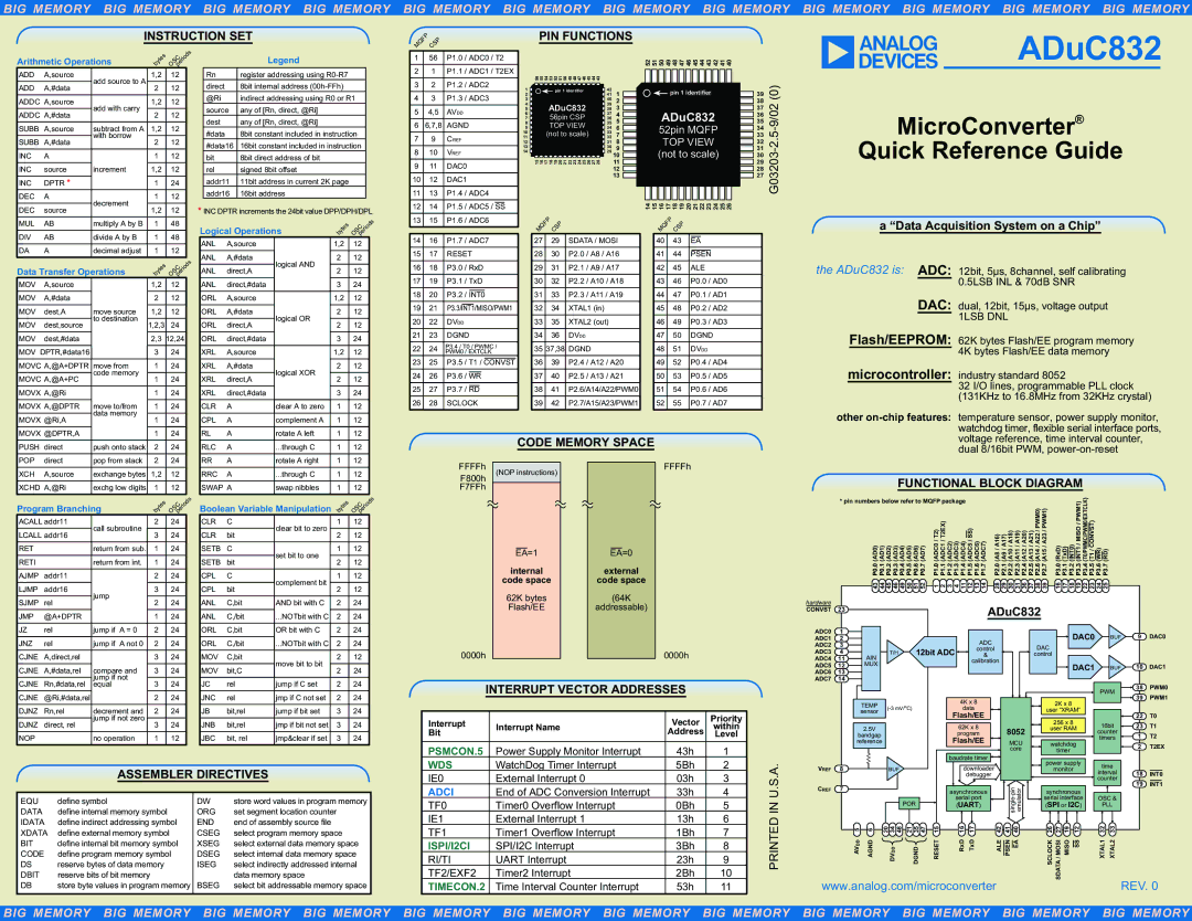
MQFP CSP | PIN FUNCTIONS |
|
ADuC832
Arithmetic Operations | bytes | OSCperiods |
| ||
ADD | A,source | add source to A | 1,2 | 12 |
|
ADD | A,#data | 2 | 12 |
| |
|
| ||||
|
|
|
|
|
|
ADDC | A,source | add with carry | 1,2 | 12 |
|
|
|
|
|
| |
ADDC | A,#data | 2 | 12 |
| |
|
| ||||
|
|
|
|
|
|
SUBB | A,source | subtract from A | 1,2 | 12 |
|
|
| with borrow |
|
|
|
SUBB | A,#data | 2 | 12 |
| |
|
| ||||
|
|
|
|
|
|
INC | A |
| 1 | 12 |
|
|
|
|
|
|
|
INC | source | increment | 1,2 | 12 |
|
|
|
|
|
|
|
INC | DPTR * |
| 1 | 24 |
|
|
|
|
|
|
|
DEC | A | decrement | 1 | 12 |
|
|
|
|
|
| |
DEC | source | 1,2 | 12 |
| |
|
| ||||
|
|
|
|
|
|
MUL | AB | multiply A by B | 1 | 48 |
|
|
|
|
|
|
|
DIV | AB | divide A by B | 1 | 48 |
|
|
|
|
|
|
|
DA | A | decimal adjust | 1 | 12 |
|
Data Transfer Operations | bytes | OSCperiods |
| ||
MOV | A,source |
| 1,2 | 12 |
|
|
|
|
|
|
|
MOV | A,#data |
| 2 | 12 |
|
|
|
|
|
|
|
MOV | dest,A | move source | 1,2 | 12 |
|
|
| to destination |
|
|
|
MOV | dest,source | 1,2,3 | 24 |
| |
|
| ||||
|
|
|
|
| |
MOV | dest,#data |
| 2,3 12,24 |
| |
|
|
|
|
| |
MOV DPTR,#data16 |
| 3 | 24 |
| |
|
|
|
| ||
MOVC A,@A+DPTR move from | 1 | 24 |
| ||
|
| code memory |
|
|
|
MOVC A,@A+PC | 1 | 24 |
| ||
|
| ||||
|
|
|
|
| |
MOVX A,@Ri |
| 1 | 24 |
| |
|
|
|
|
| |
MOVX A,@DPTR | move to/from | 1 | 24 |
| |
|
| data memory |
|
|
|
MOVX @Ri,A | 1 | 24 |
| ||
|
| ||||
|
|
|
|
| |
MOVX @DPTR,A |
| 1 | 24 |
| |
|
|
|
|
|
|
PUSH | direct | push onto stack | 2 | 24 |
|
|
|
|
|
|
|
POP | direct | pop from stack | 2 | 24 |
|
| Legend |
|
|
Rn | register addressing using |
direct | 8bit internal address |
@Ri | indirect addressing using R0 or R1 |
source | any of [Rn, direct, @Ri] |
dest | any of [Rn, direct, @Ri] |
#data | 8bit constant included in instruction |
#data16 | 16bit constant included in instruction |
bit | 8bit direct address of bit |
rel | signed 8bit offset |
addr11 | 11bit address in current 2K page |
addr16 | 16bit address |
*INC DPTR increments the 24bit value DPP/DPH/DPL
Logical Operations | bytes | OSCperiods |
| ||
ANL | A,source |
| 1,2 | 12 |
|
|
|
|
|
|
|
ANL | A,#data | logical AND | 2 | 12 |
|
|
|
|
|
| |
ANL | direct,A | 2 | 12 |
| |
|
| ||||
|
|
|
|
|
|
ANL | direct,#data |
| 3 | 24 |
|
|
|
|
|
|
|
ORL | A,source |
| 1,2 | 12 |
|
|
|
|
|
|
|
ORL | A,#data | logical OR | 2 | 12 |
|
|
|
|
|
| |
ORL | direct,A | 2 | 12 |
| |
|
| ||||
|
|
|
|
|
|
ORL | direct,#data |
| 3 | 24 |
|
|
|
|
|
|
|
XRL | A,source |
| 1,2 | 12 |
|
|
|
|
|
|
|
XRL | A,#data | logical XOR | 2 | 12 |
|
|
|
|
|
| |
XRL | direct,A | 2 | 12 |
| |
|
| ||||
|
|
|
|
|
|
XRL | direct,#data |
| 3 | 24 |
|
|
|
|
|
|
|
CLR | A | clear A to zero | 1 | 12 |
|
|
|
|
|
|
|
CPL | A | complement A | 1 | 12 |
|
|
|
|
|
|
|
RL | A | rotate A left | 1 | 12 |
|
|
|
|
|
|
|
RLC | A | ...through C | 1 | 12 |
|
|
|
|
|
|
|
RR | A | rotate A right | 1 | 12 |
|
1 56 P1.0 / ADC0 / T2 | 52 51 50 49 48 47 46 45 44 43 42 41 40 |
|
21 P1.1 / ADC1 / T2EX
|
|
|
|
|
|
|
|
|
|
|
|
|
|
|
|
| 56 55 54 53 52 51 50 49 48 47 46 45 44 43 |
|
|
|
|
|
|
|
|
|
|
|
|
|
|
|
|
|
|
|
|
|
|
| ||
3 | 2 | P1.2 | / ADC2 | 1 | 42 |
|
|
|
|
|
|
|
|
|
|
|
|
|
|
|
|
|
|
|
|
| (0) | |||||||||||||||
| pin 1 identifier |
|
|
|
|
|
|
|
|
|
|
|
|
|
|
|
|
|
|
|
|
| ||||||||||||||||||||
| 1 |
|
|
|
|
|
| pin 1 identifier |
| 39 | ||||||||||||||||||||||||||||||||
|
|
|
|
|
|
|
|
|
|
|
|
|
|
|
|
|
|
|
|
|
|
|
| |||||||||||||||||||
4 | 3 | P1.3 | / ADC3 | 2 |
|
|
| 41 |
|
|
|
|
|
|
|
| ||||||||||||||||||||||||||
3 |
|
|
| 40 | 2 |
|
|
|
|
|
|
|
|
|
|
|
|
|
|
|
|
|
|
| 38 | 9/02- | ||||||||||||||||
|
|
|
|
|
|
|
|
|
|
|
|
|
|
|
| 4 |
| ADuC832 | 39 | 3 |
|
|
|
|
|
|
|
|
|
|
|
|
|
|
|
|
|
|
| 37 | ||
6 | 6,7,8 | AGND | 5 |
| 38 |
|
|
|
|
|
|
|
|
|
|
|
|
|
|
|
|
|
|
| ||||||||||||||||||
9 |
| TOP VIEW | 34 | 6 |
|
|
|
|
|
|
|
|
|
|
|
|
|
|
|
|
|
|
| 34 | ||||||||||||||||||
5 | 4,5 | AVDD |
|
|
|
|
|
|
|
|
|
|
|
| 6 |
| 56pin CSP | 37 | 4 |
|
|
|
|
| ADuC832 |
| 36 |
| ||||||||||||||
|
|
|
|
|
|
|
|
|
|
|
|
|
|
|
| 8 |
| 35 |
|
|
|
|
|
| 35 |
| ||||||||||||||||
|
|
|
|
|
|
|
|
|
|
|
|
|
|
|
| 7 |
| 36 | 5 |
|
|
|
|
| 52pin MQFP |
|
| 2.5- | ||||||||||||||
|
|
|
|
|
|
|
|
|
|
|
|
|
|
|
| 10 |
| (not to scale) | 33 | 7 |
|
|
|
|
|
| 33 | |||||||||||||||
|
|
|
|
|
|
|
|
|
|
|
|
|
|
|
|
|
|
|
|
|
| |||||||||||||||||||||
7 | 9 | CREF |
|
|
|
|
|
|
|
|
|
|
|
| 11 |
| 32 |
|
|
|
|
|
| TOP VIEW |
| |||||||||||||||||
|
|
|
|
|
|
|
|
|
|
|
| 13 |
|
|
| 30 | 9 |
|
|
|
|
|
| 31 | ||||||||||||||||||
|
|
|
|
|
|
|
|
|
|
|
|
|
|
|
| 12 |
|
|
| 31 | 8 |
|
|
|
|
| (not to scale) |
| 32 |
| ||||||||||||
|
|
|
|
|
|
|
|
|
|
|
|
|
|
|
|
|
|
|
|
|
|
|
|
|
|
|
|
|
| |||||||||||||
8 | 10 | VREF |
|
|
|
|
|
|
|
|
|
|
|
| 14 |
|
|
| 29 10 |
|
|
|
|
|
| 30 | G03203 | |||||||||||||||
|
|
|
|
|
|
|
|
|
|
|
|
|
|
|
|
| 15 16 17 18 19 20 21 22 23 24 25 26 27 28 |
| 11 |
|
|
|
|
|
|
|
|
|
|
|
|
|
|
|
|
|
|
| 29 | |||
9 | 11 | DAC0 |
|
|
|
|
| 12 |
|
|
|
|
|
|
|
|
|
|
|
|
|
|
|
|
|
|
| 28 |
| |||||||||||||
|
|
|
|
|
|
|
|
|
|
|
|
|
|
|
|
|
|
|
|
| 13 |
|
|
|
|
|
|
|
|
|
|
|
|
|
|
|
|
|
|
| 27 |
|
10 | 12 | DAC1 |
|
|
|
|
|
|
|
|
|
|
|
|
|
|
|
|
|
|
|
|
|
|
|
|
|
|
| |||||||||||||
|
|
|
|
|
|
|
|
|
|
|
|
|
|
|
|
|
|
|
|
|
|
|
|
|
|
|
|
|
|
|
|
|
|
|
|
|
|
|
|
|
|
|
11 | 13 | P1.4 | / ADC4 |
|
|
|
|
|
|
|
|
|
|
|
|
|
|
|
|
|
|
|
|
|
|
|
|
|
|
| ||||||||||||
|
|
|
|
|
|
|
|
|
|
|
|
|
|
|
|
|
|
|
|
|
|
|
|
|
|
|
|
|
|
|
|
|
|
|
|
|
|
|
|
|
|
|
12 | 14 | P1.5 | / ADC5 / |
|
|
|
|
|
|
|
|
|
|
|
|
|
|
|
|
|
|
|
|
|
|
|
|
|
|
|
|
|
| |||||||||
SS |
|
|
|
|
|
|
|
| 14 15 16 17 18 19 20 21 22 23 24 25 26 |
|
|
|
| |||||||||||||||||||||||||||||
13 | 15 | P1.6 | / ADC6 |
| MQFP | CSP |
|
|
|
|
|
|
|
| MQFP CSP |
|
|
|
|
|
|
|
|
|
|
| ||||||||||||||||
|
|
|
|
|
|
|
|
|
|
|
|
|
|
|
|
|
|
|
|
|
|
|
|
|
|
|
|
|
|
|
|
|
|
|
| |||||||
14 | 16 | P1.7 | / ADC7 |
| 27 | 29 | SDATA / MOSI |
|
| 40 | 43 |
| EA |
|
|
|
|
|
|
|
|
| ||||||||||||||||||||
15 | 17 | RESET |
| 28 | 30 | P2.0 / A8 / A16 |
|
| 41 | 44 |
|
|
|
|
|
|
|
|
|
|
|
| ||||||||||||||||||||
|
|
| PSEN |
|
|
| ||||||||||||||||||||||||||||||||||||
16 | 18 | P3.0 | / RxD |
| 29 | 31 | P2.1 / A9 / A17 |
|
| 42 | 45 |
| ALE |
|
|
| ||||||||||||||||||||||||||
|
|
|
|
|
|
|
|
|
|
|
|
|
|
|
|
|
|
|
|
|
|
|
|
|
|
|
|
|
|
|
|
|
|
|
|
|
|
|
|
| ||
17 | 19 | P3.1 | / TxD |
| 30 | 32 | P2.2 / A10 / A18 |
|
| 43 | 46 |
| P0.0 / AD0 |
|
|
| ||||||||||||||||||||||||||
|
|
|
|
|
|
|
|
|
|
|
|
|
|
|
|
|
|
|
|
|
|
|
|
|
|
|
|
|
|
|
|
|
|
|
|
|
|
|
|
| ||
18 | 20 | P3.2 | / |
|
|
|
|
|
|
|
|
|
| 31 | 33 | P2.3 / A11 / A19 |
|
| 44 | 47 |
| P0.1 / AD1 |
|
|
| |||||||||||||||||
INT0 |
|
|
|
|
|
| ||||||||||||||||||||||||||||||||||||
19 | 21 |
|
|
|
|
|
|
|
|
|
| 32 | 34 | XTAL1 (in) |
|
|
|
|
|
| 45 | 48 |
| P0.2 / AD2 |
|
|
| |||||||||||||||
P3.3/INT1/MISO/PWM1 |
|
|
|
|
|
|
|
|
|
| ||||||||||||||||||||||||||||||||
20 | 22 | DVDD |
|
|
|
|
|
|
|
|
|
|
|
|
| 33 | 35 | XTAL2 (out) |
|
|
|
|
| 46 | 49 |
| P0.3 / AD3 |
|
|
| ||||||||||||
|
|
|
|
|
|
|
|
|
|
|
|
|
|
|
|
|
|
|
|
|
|
|
|
|
|
|
|
|
|
|
|
|
|
|
|
|
|
|
|
|
| |
21 | 23 | DGND |
| 34 | 36 | DVDD |
|
|
|
|
|
| 47 | 50 |
| DGND |
|
|
| |||||||||||||||||||||||
|
|
|
|
|
|
|
|
|
|
|
|
|
|
|
|
|
|
|
|
|
|
|
|
|
|
|
|
|
|
|
|
|
|
|
|
|
|
|
|
|
| |
22 | 24 | P3.4 / T0 / PWMC / |
| 35 | 37,38 | DGND |
|
|
|
|
|
| 48 | 51 |
| DVDD |
|
|
| |||||||||||||||||||||||
|
| PWM0 / EXTCLK |
|
|
|
|
|
|
|
|
|
|
|
|
|
|
|
|
|
|
|
|
|
|
|
|
|
|
| |||||||||||||
23 | 25 | P3.5 | / T1 / |
|
|
| 36 | 39 | P2.4 / A12 / A20 |
|
| 49 | 52 |
| P0.4 / AD4 |
|
|
| ||||||||||||||||||||||||
CONVST |
|
|
|
|
|
| ||||||||||||||||||||||||||||||||||||
24 | 26 | P3.6 | / |
|
|
|
|
| 37 | 40 | P2.5 / A13 / A21 |
|
| 50 | 53 |
| P0.5 / AD5 |
|
|
| ||||||||||||||||||||||
WR |
|
|
|
|
|
| ||||||||||||||||||||||||||||||||||||
25 | 27 | P3.7 | / |
|
|
| 38 | 41 | P2.6/A14/A22/PWM0 |
|
| 51 | 54 |
| P0.6 / AD6 |
|
|
| ||||||||||||||||||||||||
RD |
|
|
|
|
|
| ||||||||||||||||||||||||||||||||||||
26 | 28 | SCLOCK |
| 39 | 42 | P2.7/A15/A23/PWM1 |
|
| 52 | 55 |
| P0.7 / AD7 |
|
|
| |||||||||||||||||||||||||||
CODE MEMORY SPACE
MicroConverter®
Quick Reference Guide
a “Data Acquisition System on a Chip”
the ADuC832 is: ADC: 12bit, 5µs, 8channel, self calibrating 0.5LSB INL & 70dB SNR
DAC: dual, 12bit, 15µs, voltage output
1LSB DNL
Flash/EEPROM: 62K bytes Flash/EE program memory 4K bytes Flash/EE data memory
microcontroller: industry standard 8052
32 I/O lines, programmable PLL clock (131KHz to 16.8MHz from 32KHz crystal)
other
XCH | A,source | exchange bytes | 1,2 | 12 |
| |
|
|
|
|
|
| |
XCHD | A,@Ri | exchg low digits | 1 | 12 |
| |
Program Branching |
| bytes | OSCperiods |
| ||
ACALL addr11 | call subroutine | 2 | 24 |
| ||
|
|
|
|
| ||
LCALL addr16 | 3 | 24 |
| |||
|
|
| ||||
|
|
|
|
|
| |
RET |
| return from sub. | 1 | 24 |
| |
|
|
|
|
|
| |
RETI |
| return from int. | 1 | 24 |
| |
|
|
|
|
|
|
|
AJMP | addr11 |
|
| 2 | 24 |
|
|
|
|
|
|
|
|
LJMP | addr16 | jump |
| 3 | 24 |
|
|
|
|
|
|
| |
SJMP | rel |
| 2 | 24 |
| |
|
|
| ||||
|
|
|
|
|
|
|
JMP | @A+DPTR |
|
| 1 | 24 |
|
|
|
|
|
|
|
|
JZ | rel | jump if | A = 0 | 2 | 24 |
|
|
|
|
|
|
|
|
JNZ | rel | jump if | A not 0 | 2 | 24 |
|
|
|
|
|
|
|
|
CJNE | A,direct,rel |
|
| 3 | 24 |
|
|
|
|
|
|
| |
CJNE | A,#data,rel | compare and | 3 | 24 |
| |
|
| jump if not |
|
|
| |
CJNE | Rn,#data,rel | equal |
| 3 | 24 |
|
CJNE | @Ri,#data,rel |
|
| 2 | 24 |
|
|
|
|
|
|
| |
DJNZ | Rn,rel | decrement and | 2 | 24 |
| |
|
| jump if not zero |
|
|
| |
DJNZ | direct, rel | 3 | 24 |
| ||
|
|
| ||||
|
|
|
|
|
| |
NOP |
| no operation | 1 | 12 |
| |
RRC | A | ...through C | 1 | 12 |
| |
|
|
|
|
| ||
SWAP A | swap nibbles | 1 | 12 |
| ||
Boolean Variable Manipulation | bytes | OSCperiods |
| |||
CLR | C | clear bit to zero |
| 1 | 12 |
|
|
|
|
|
|
| |
CLR | bit |
| 2 | 12 |
| |
|
|
| ||||
|
|
|
|
|
|
|
SETB | C | set bit to one |
| 1 | 12 |
|
|
|
|
|
|
| |
SETB | bit |
| 2 | 12 |
| |
|
|
| ||||
|
|
|
|
|
|
|
CPL | C | complement bit |
| 1 | 12 |
|
|
|
|
|
|
| |
CPL | bit |
| 2 | 12 |
| |
|
|
| ||||
|
|
|
|
|
|
|
ANL | C,bit | AND bit with C |
| 2 | 24 |
|
|
|
|
|
|
|
|
ANL | C,/bit | ...NOTbit with C |
| 2 | 24 |
|
|
|
|
|
|
|
|
ORL | C,bit | OR bit with C |
| 2 | 24 |
|
|
|
|
|
|
|
|
ORL | C,/bit | ...NOTbit with C |
| 2 | 24 |
|
|
|
|
|
|
|
|
MOV | C,bit | move bit to bit |
| 2 | 12 |
|
|
|
|
|
|
| |
MOV | bit,C |
| 2 | 24 |
| |
|
|
| ||||
|
|
|
|
|
|
|
JC | rel | jump if C set |
| 2 | 24 |
|
|
|
|
|
|
|
|
JNC | rel | jmp if C not set |
| 2 | 24 |
|
|
|
|
|
|
|
|
JB | bit,rel | jump if bit set |
| 3 | 24 |
|
|
|
|
|
|
|
|
JNB | bit,rel | jmp if bit not set |
| 3 | 24 |
|
|
|
|
|
|
|
|
JBC | bit, rel | jmp&clear if set |
| 3 | 24 |
|
FFFFh | (NOP instructions) |
| FFFFh |
|
|
|
|
|
|
|
|
|
|
|
|
|
F800h |
|
|
|
|
| FUNCTIONAL BLOCK DIAGRAM |
|
|
| |||||||
|
|
|
|
|
|
|
|
| ||||||||
F7FFh |
|
|
|
|
|
|
|
|
| |||||||
|
|
|
|
| * pin numbers below refer to MQFP package |
|
| ) |
|
|
| |||||
|
|
|
|
|
|
| (RxD) (TxD) (INT0) (INT1 / MISO / PWM1) (T0/PWMC/PWM0/EXTCLK (T1 / CONVST) (WR) (RD) |
|
| |||||||
| EA=1 | EA=0 |
|
|
| (AD0) (AD1) (AD2) (AD3) (AD4) (AD5) (AD6) (AD7) | (ADC0 / T2) (ADC1 / T2EX) (ADC2) (ADC3) (ADC4) (ADC5 / SS) (ADC6) (ADC7) | (A8 / A16) | (A9 / A17) (A10 / A18) (A11 / A19) (A12 / A20) (A13 / A21) (A14 / A22 / PWM0) (A15 / A23 / PWM1) |
|
| |||||
|
|
|
|
|
|
|
| |||||||||
| internal | external |
|
|
| P0.0 P0.1 P0.2 P0.3 P0.4 P0.5 P0.6 P0.7 | P1.0 P1.1 P1.2 P1.3 P1.4 P1.5 P1.6 P1.7 | P2.0 P2.1 P2.2 P2.3 P2.4 P2.5 P2.6 P2.7 | P3.0 P3.1 P3.2 P3.3 P3.4 P3.5 P3.6 P3.7 |
|
| |||||
| code space | code space |
|
|
| 43 44 45 46 49 50 51 52 | 1 2 3 4 | 11 12 13 14 | 28 29 30 31 36 37 38 39 | 16 17 18 19 22 23 24 25 |
|
| ||||
|
|
|
|
|
|
|
| |||||||||
| 62K bytes | (64K |
| hardware |
|
|
|
|
|
|
|
|
|
|
|
|
| Flash/EE | addressable) |
|
|
|
|
|
|
| ADuC832 |
|
|
|
| ||
|
| CONVST | 23 |
|
|
|
|
|
|
|
|
| ||||
|
|
|
| ADC0 | 1 |
|
|
|
|
|
|
| DAC0 | BUF | 9 | DAC0 |
|
|
|
| ADC1 | 2 |
|
|
|
| ADC |
| |||||
|
|
|
| ADC2 | 3 |
|
|
|
| DAC |
|
|
|
| ||
|
|
|
|
|
| 12bit ADC | control |
|
|
|
| |||||
0000h |
|
| 0000h | ADC3 | 4 |
| T/H |
|
|
|
| |||||
|
| AIN | & |
| control |
|
|
| ||||||||
|
| ADC4 | 11 |
|
|
|
|
| ||||||||
|
|
|
| ADC5 | 12 | MUX |
|
|
| calibration |
| DAC1 |
| 10 | DAC1 | |
|
|
|
|
|
|
|
|
|
| BUF | ||||||
|
|
|
| ADC6 | 13 |
|
|
|
|
|
|
|
|
|
|
|
INTERRUPT VECTOR ADDRESSES | ADC7 | 14 |
|
|
|
|
|
|
|
|
|
|
| |||
|
|
|
|
|
|
|
|
|
| PWM | 38 | PWM0 | ||||
|
|
|
|
|
|
|
|
|
| 39 | PWM1 | |||||
|
|
|
|
|
|
|
|
|
| 4K x 8 |
|
| 2K x 8 |
| ||
|
|
|
|
|
| TEMP | o |
|
|
|
|
|
|
| ||
|
|
|
|
|
|
|
| data |
|
|
|
|
| |||
|
|
|
|
|
| sensor | C) |
|
| user “XRAM” |
| 22 | T0 | |||
Interrupt |
|
| Vector | Priority |
|
|
|
| Flash/EE |
|
| 256 x 8 |
| |||
Interrupt Name |
| within |
| 2.5V |
|
| 62K x 8 |
|
| 16bit | 23 | T1 | ||||
| Address |
|
|
|
| 8052 | user RAM | |||||||||
Bit |
|
| Level |
| bandgap |
|
| program |
|
| counter | 1 | T2 | |||
|
|
|
|
|
| reference |
|
| Flash/EE |
| MCU | watchdog | timers | |||
PSMCON.5 | Power Supply Monitor Interrupt | 43h | 1 |
|
|
|
|
| 2 | T2EX | ||||||
|
|
|
|
|
|
| core | timer |
| |||||||
|
|
|
|
|
|
|
|
|
| |||||||
|
|
|
| baudrate timer |
|
|
|
|
| |||||||
WDS | WatchDog Timer Interrupt | 5Bh | 2 |
|
|
|
| power supply |
|
|
| |||||
|
|
|
|
|
|
| time |
|
| |||||||
ASSEMBLER DIRECTIVES
| EQU | define symbol | DW | store word values in program memory |
|
| DATA | define internal memory symbol | ORG | set segment location counter |
|
| IDATA | define indirect addressing symbol | END | end of assembly source file |
|
| XDATA | define external memory symbol | CSEG | select program memory space |
|
| BIT | define internal bit memory symbol | XSEG | select external data memory space |
|
| CODE | define program memory symbol | DSEG | select internal data memory space |
|
| DS | reserve bytes of data memory | ISEG | select indirectly addressed internal |
|
| DBIT | reserve bits of bit memory |
| data memory space |
|
| DB | store byte values in program memory | BSEG | select bit addressable memory space |
|
|
|
|
| ||
BIG MEMORY BIG MEMORY | BIG MEMORY BIG MEMORY | ||||
|
|
|
| IN U.S.A. | VREF | 8 |
| BUF |
| downloader |
|
| monitor | interval | 18 | INT0 |
IE0 | External Interrupt 0 | 03h | 3 |
|
|
|
|
| debugger |
|
|
| ||||
|
|
|
|
|
|
|
|
| counter | 19 | INT1 | |||||
ADCI | End of ADC Conversion Interrupt | 33h | 4 | CREF | 7 |
|
|
|
|
|
|
| ||||
|
|
| asynchronous |
| synchronous |
|
|
| ||||||||
|
|
|
|
|
| OSC & |
|
| ||||||||
TF0 | Timer0 Overflow Interrupt | 0Bh | 5 |
|
|
|
| POR | serial port |
| serial interface |
|
| |||
|
|
|
| (UART) |
| (SPI or I2C) | PLL |
|
| |||||||
|
|
|
|
|
|
|
| |||||||||
IE1 | External Interrupt 1 | 13h | 6 |
|
|
|
|
|
|
|
|
|
|
| ||
PRINTED |
|
|
|
|
|
|
|
|
|
|
|
| ||||
TF1 | Timer1 Overflow Interrupt | 1Bh | 7 |
| 5 |
| 34 | 21 DGND 35 47 RESET 15 | RxD 16 TxD 17 | ALE 42 | PSEN 41 EA 40 | SCLOCK 26 SDATA/ MOSI 27 MISO 19 SS 12 | XTAL1 32 XTAL2 33 |
|
| |
|
|
|
|
|
| |||||||||||
ISPI/I2CI | SPI/I2C Interrupt | 3Bh | 8 |
| DD |
| DD |
|
| |||||||
|
|
|
|
| ||||||||||||
RI/TI | UART Interrupt | 23h | 9 |
| AV | AGND6 | 20 DV 48 |
|
| |||||||
TF2/EXF2 | Timer2 Interrupt | 2Bh | 10 |
| REV. 0 | |||||||||||
TIMECON.2 | Time Interval Counter Interrupt | 53h | 11 |
| www.analog.com/microconverter |
|
|
| ||||||||
BIG MEMORY | BIG MEMORY BIG MEMORY | BIG MEMORY | BIG MEMORY | BIG MEMORY |
| BIG MEMORY | BIG MEMORY | |||||||||