D

6

JK85

CJJ4M069Z(GOLD)


Z2 OUT


C770

68

C769

68P

470/10V

R825


VGND

VGND


5

4

3

2

1


VIDEO PART

D


C806

0.01uF


C827

1/50V


6

5


C805

0.01uF


1


C

3


C826

1/50V

VCR


Y

4

R804

75

R805

75

R806

75

C804

0.01uF


2


JK81

7


VGND

VGND

VGND

C825

1/50V


8


CJJ9P004Z(GOLD)

17


13


C803

0.01uF


9


C

11


Y

12


C824

1/50V

AV


10


C802

0.01uF


15


16


C823

1/50V


14


C801

0.01uF


VGND


C822


R801

75

R802

75

R803

75

1/50V


VGND

VGND

VGND


6

5


C812

0.01uF


1


C

3


SAT

Y

4


C833

1/50V


2


C811

0.01uF


7


Y2

Pb4


38

37

36

39

V+

Y4

40Pr4

41V+

42Y3

44Pb3

45V+

46Pr3

47

V+

Pb2


48

1

2


AUX1

AUX0

PbOUT2


35

34

33

32

31

30

29

28

27


26

25

24


V+

OUTY


OUTPb


OUTPr

AUX3

AUX2

OUT2Y

PORT1


PORT0

23


22


Pr_OUT2

21


IC81


V+

20


VREF


NJW1321FP1


DGND

18


19


GND

17


SDA

16

VGND


Pr2


Pb1


Pr1


Y1

V+

V+


SCL

15


3

4

5

6

7

8

9


10

11

12

13

14


PORT3

PORT2

ADR

47K


R833


+9VV

C834

10/50 C836

0.1uF

100/16


C835

VGND

VGND

VGND


R831

33


R832

33

+5VV


C868

0.1uF

100/16


VGND


C869


HVINJM2244MTE1

8

7

6

5


Vin1GND

VOUTSW1

V+Vin2

Vin3SW2


VGND

VGND

IC85


1

2

3

4


VGND


VGND


R8611M

C865

C866

0.01uF

R8631M

C867

0.01uF


R8621M


10/50V


VGND


VGND

VGND


VGND

VGND


* LC74763M OPTION TABLE


+5VV


C871


C872


X801

X802


PAL

27P


27P


17.734

14.318


NTSC

27P


27P


14.318

X


X801


VGND


17.734MHz(EU)


C871


27P

C872


27P


VGND


VGND


X802


14.318MHz


C873

(EU)


C874


(EU)


27P


27P


OSD_CE1


VGND


VGND


OSD_DA


OSD_CLK


1K

1K

1K


C888


180P R884

R883

R882


VGND


VGND


C887


0.47/50


VGND


L801


100UH


C876

0.022u C875

100/16


100K


IC83

LC74763MIC83

R886


LC74763M


1

VSS

30


VGND

VGND

VGND


VDD1


R871


Xin1

29


2


SYNCDET


1K


3

Xout1

28


L802


0.022u


VCOOUT


C840VGND1uF

HSYNCOUT


C880

5.6UH

-22P>33P


5 4

FC

26 27


22P

C879


C878VGND


VCOIN


Xin2


Xout2

25


VGND

VGND


R872


6


AMPOUT


R873


1K


7

VSYNCOUT

24


1K


AMPIN


C881


R874


8

notCS

23


1/50 C882

6.8K


PDOUT


R875


9

SIN

22


1.5K


6800P


AMPIN


10

SCLK

21


R876


PDOUT

VGND


C883 39K


11

SECAM

20


SYNCIN


0.1/50

C884


R877

2.2K C885

22P

12

CVCR

19


not525/625


56P


13

notNTSC/PAL

18


CVIN


VGND


14

not3.58/4.43

17


R885

270


VDD2


15

notRST

16


CVOUT


Q802


VGND


R878

10K C886

22P


KTC3875SY


R880

0


R879

8.2K


VGND


VGND

C


JK82

8


CJJ9P004Z(GOLD)

17

R810


R811


R812


C832

1/50V


13

75

75

75

C810

0.01uF


9


C

11


C831

1/50V

BD

Y

12

VGND

VGND

VGND


10


C809

0.01uF


15


16


R866

100K


COMPO OSD IN


470/10


+9VV


COMPO OUT

C890

C889


R881

R867

OPEN

10/50


1.2K


+5VV


Q801

R868

2.2K

C

B


14


C830

1/50V


C808

0.01uF


VGND


C829


1/50V


C807

0.01uF


R807

75 R808

75 R809

75

C828

1/50V


VGND

VGND

VGND


JK83


9

Pr3


C813

0.01uF


IN3


R813

75

C751

2P

C771

1/50V


8


AV

& COMPONENT CJJ4R046Z(GOLD)

7

Pr2

VGND

VGND

C816

0.01uF


R816

75

C754

2P

C774

1/50V


6

Pb3

VGND

VGND

C814

0.01uF


R814

75

C752

2P

C772

1/50V


5


4

Pb2

VGND

VGND

C817

0.01uF


IN2


R817

75

C755

2P

C775

1/50V


COMPONENT

3

Y3

VGND

VGND

C815

0.01uF


BD


R815

75


2P

C773

1/50V


2


Y2


VGND

C818

0.01uF


1

VGND

C756C753


R818

75

2P

C776

1/50V


1,4,7 : UPPER


3,6,9 : LOWER


VGND


VGND

VGND


JK84


C819

0.01uF


Pr1


IN1

9


R819

75

C760

2P

C766

1/50V


SAT

8


VGND

VGND


C765

Y2

Pb4


38

37

36

39

V+

Y4

40Pr4

41V+

42Y3

44Pb3

45V+

46Pr3

47

V+

Pb2


48

1

2


J1

J2


J3

J7


AUX4

AUX3


AUX2

AUX1


AUX1

AUX0


PbOUT2


35

34

33

32

31

30

29

28

27

26

25

24


V+

OUTY


OUTPb


OUTPr

AUX3

AUX2

OUT2Y

PORT1


PORT0


23


22


Pr_OUT2


21


IC82


V+

20


NJW1321FP1


VREF


19


DGND

18


GND


17


SDA


16

VGND


Pr2


Pb1


Pr1


Y1

V+

V+


SCL


15


3

4

5

6

7

8

9


10

11

12

13

14


PORT3

PORT2


ADR


VGND

+5VV


C841


C857

100/16V

1

IC84 CVINJM2566V

32


1

S1

32


R844


PS1


S-C

10K


0.01uF


2

2

SCIN

31

31


S2


C847

10/50V


3

V+1

30


3

SDCOUT

30


C853


4

4

NC-0

29

29


SCOUT


0.1uF


C842


5

5

MIXSW

28

28


NC-3


0.01uF

CVBS


6

6

VIN

27

27


VOUT


C848

10/50V


7

GND1

26


C843


7

V+4

26


0.01uF

S-Y


8

8

SYIN

25

25

C855


SYOUT


C849

10/50V


R841


9

CBSW

24


0.1uF


C844

Y

4.7K


9

GND4

24


10

YIN

23


0.01uF


10

23


YOUT


C850

10/50V


11

V+2

22


11

22


V+3


C854


12

12

NC-1

21

21

C856


PBOUT


0.1uF


GND2


0.1uF


C845


13

13

20

20


NC-2


0.01uF

Pb


14

14

PBIN

19

19


R842


GND3


C851

10/50V


15

PS2

18


C846


10K


15

PROUT

18

R843


Pr


0.01uF


16

16

PRIN

17

17


LPFSW

4.7K


C852

10/50V


+9VV


VGND

C837

10/50 C838

0.1uF

100/16


C839


VGND VGND

VGND


R834

33


R835

33


C858 75

470/10V R845

C859 75

470/10V R846

C860 75

470/10V R847

C861 75

470/10V R848

C862 75

470/10V R849

C863

75

470/10V

R850

VGND

VGND

KTA1504SY


VGND

VGND


D801


OSD_CE1


OSD_CLK


8

9

10

11

12

13

14

C891

0.022u


IC86


VGND


7

6

5

4

3

2

1

IC86


VGND


SN74ACT0DR


OSD_DA

R887

1K

OSD_SDA


OSD_CE1


R888

1K

OSD_SCL


R889

1K

OSD_CE


J9

+15VV -5VA

CN301

1

2

3

4

5

6

7

8

9

10

11

12

13

14

15

16

17

18

19

20

21

22

23

24

25

26

27

28

29

30

+15VA -5VA

VGND

OSD_H

SV_Y_THURE SV_C_THURE CVBS_THURE VGND COM_Y_THURE COM_Pb_THURE COM_Pr_THURE VGND COM_Y_CONV COM_Pb_CONV COM_Pr_CONV VGND

1321_SCL

1321_SDA

OSD_DATA

OSD_CLK

OSD_CE

VGND

N.D

N.D

N.D

VGND

N.D

N.D

N.D

N.D

To HDMI B'D

B

MONITOROUT COMPONENTOUT & COMPONENT


7

Pr_OUT


75


C762C758 C761C757

2P


R822

1000/6.3


Pb1


VGND

C820

0.01uF


CJJ4R046Z(GOLD)

6


R820

75

2P

C767

1/50V


5


4

Pb_OUT

VGND

VGND


75

C764


2P


R823

1000/6.3


Y1


VGND

C821

0.01uF


3


R821

75

2P

C768

1/50V


2


Pr_OUT

Pb_OUT

Y_OUT

* DEFINITION OF I2C REGISTER ( NJW1321 )

I2C BUS FORMAT


+15VV

+5VV

+9VV


IC89


IC88


N.D


CVIKIA1117S50


CVIKIA7809AF


CVD1N4003SRT


L803


L804


2

Out In 3


3


1


D802


10uH


10uH

OUT IN


C897

10/50V

C896

0.1uF


GND

C895

0.1uF

C894

10/50V


GND

0.1uF

C893

C892

10/50V


1


2

VGND

A


1

Y_OUT

VGND

VGND

75

C763


VGND


C759

2P

R824

1000/6.3


1,4,7

: UPPER


3,6,9

: LOWER


VGND


MSB

LSB


MSB

LSB


MSB


LSB


S : Starting Term


A : Acknowledge Bit

S(1BIT)


SLAVE ADDRESS(8BIT)


A(1BIT)

DATA(8BIT)


A(1BIT)


DATA(8BIT)

A(1BIT)


P(1BIT)


P : Ending Term

SLAVE ADDRESS


MSB


Slave Address(8BIT)


MSB


Hex

R/NOT W : Set the Write Mode or Read Mode.


ADR : Set the Slave Address by " ADR" terminal.

1


0


0


0

0


0


ADR(1BIT)


R/NOT W(1BIT)


-


CONTROL REGISTER TABLE


R/NOT W = 0 : WRITE MODE, ADR = 0/1 ; ADR=0 Hex:94(h), ADR=1 Hex:96(h)


R/NOT W = 0 : READ MODE, ADR = 0/1 ; ADR=0 Hex:95(h), ADR=1 Hex:97(h)

<WRITE MODE>


NO.


BIT


PS : POWER SAVE


D7


D6

D5


D4


D3


D2


D1


D0

=> PS = 1 ; POWER SAVE ON (MUTE), PS = 0 ; POWER SAVE OFF (OUT ON)


DATA 1


PS1


PS2


OUT1


OUT2


OUT : OUTPUT

DATA 2


AUX0


AUX1


AUX2


AUX3


AUX : AUXILIARY (CONTROL SIGNAL OUTPUT)

<READ MODE>


NO.


BIT


D7


D6

D5


D4


D3


D2


D1


D0


DATA


PORT0


PORT1


PORT2


PORT3


PORT : INPUT


VGND


REVISION

2


4


6


1


3


5


7


A


SCHEMATIC DIAGRAM

SHEET


MODEL


AVR400

13

15


MP


DESIGN

CHECK

APPROVE


DRAWING NO


L.J.Y

L.J.H

S.H.S


2330SCDZ


(VIDEO)


10.11.17

10.11.17


10.11.17


1

3


Page 32
Image 32
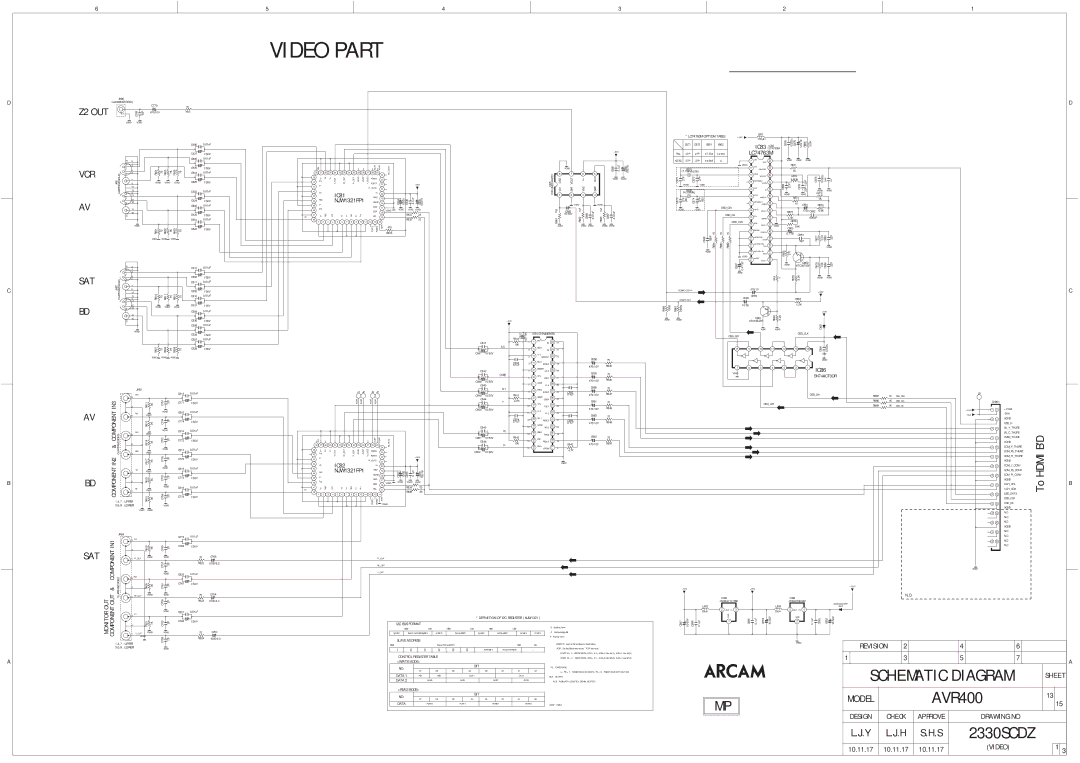
Arcam AVR400 service manual IC81, IC83, LC74763M, IC82 NJW1321FP1, IC86

AVR400 specifications

The Arcam AVR400 is a high-performance AV receiver designed to provide an immersive home theater experience. As part of Arcam’s esteemed lineup, the AVR400 combines advanced technology with exceptional sound quality, catering to audiophiles and home cinema enthusiasts alike.

At the heart of the AVR400 is its impressive power amplification, providing 100 watts per channel across 7 channels, ensuring a robust performance capable of driving a wide range of speakers. This power output is complemented by a high-current design, which means the receiver can handle dynamic audio passages without distortion, offering clarity in both subtle and explosive soundtracks.

One of the standout features of the AVR400 is its support for various surround sound formats, including Dolby TrueHD and DTS-HD Master Audio. This allows for an unparalleled audio experience, transporting users right into the heart of the action. Additionally, the AVR400 is equipped with the latest HDMI inputs, ensuring compatibility with a multitude of high-definition sources, including Blu-ray players, gaming consoles, and streaming devices.

The AVR400 also boasts advanced video processing capabilities, supporting 4K pass-through as well as upscaling of lower-resolution content to 4K. This makes it an ideal choice for users looking to future-proof their home theater setup, as it can seamlessly integrate with modern 4K televisions while enhancing the quality of older content.

User-friendliness is another essential characteristic of the Arcam AVR400. It comes equipped with an intuitive on-screen menu system that simplifies the setup process. The inclusion of an automatic calibration system helps optimize speaker settings in accordance with the room acoustics, ensuring users achieve the best sound possible from their setup.

Furthermore, the network features of the AVR400 allow for streaming audio from various online services and wireless devices. Built-in support for DLNA enables users to access their media library wirelessly, while the USB input allows for direct playback from flash drives or external hard drives.

In terms of build quality, the Arcam AVR400 embodies the brand’s commitment to excellence. With a sleek design, high-quality materials, and an engineered chassis that minimizes vibration and interference, the AVR400 is not only visually appealing but also built to deliver performance over time.

In summary, the Arcam AVR400 is a feature-rich AV receiver offering a perfect blend of power, precision, and versatility. Whether for movie nights or music listening, it stands out as a reliable choice for those seeking high-quality audio and video reproduction in their home entertainment systems.