AT90S8515-4 specifications
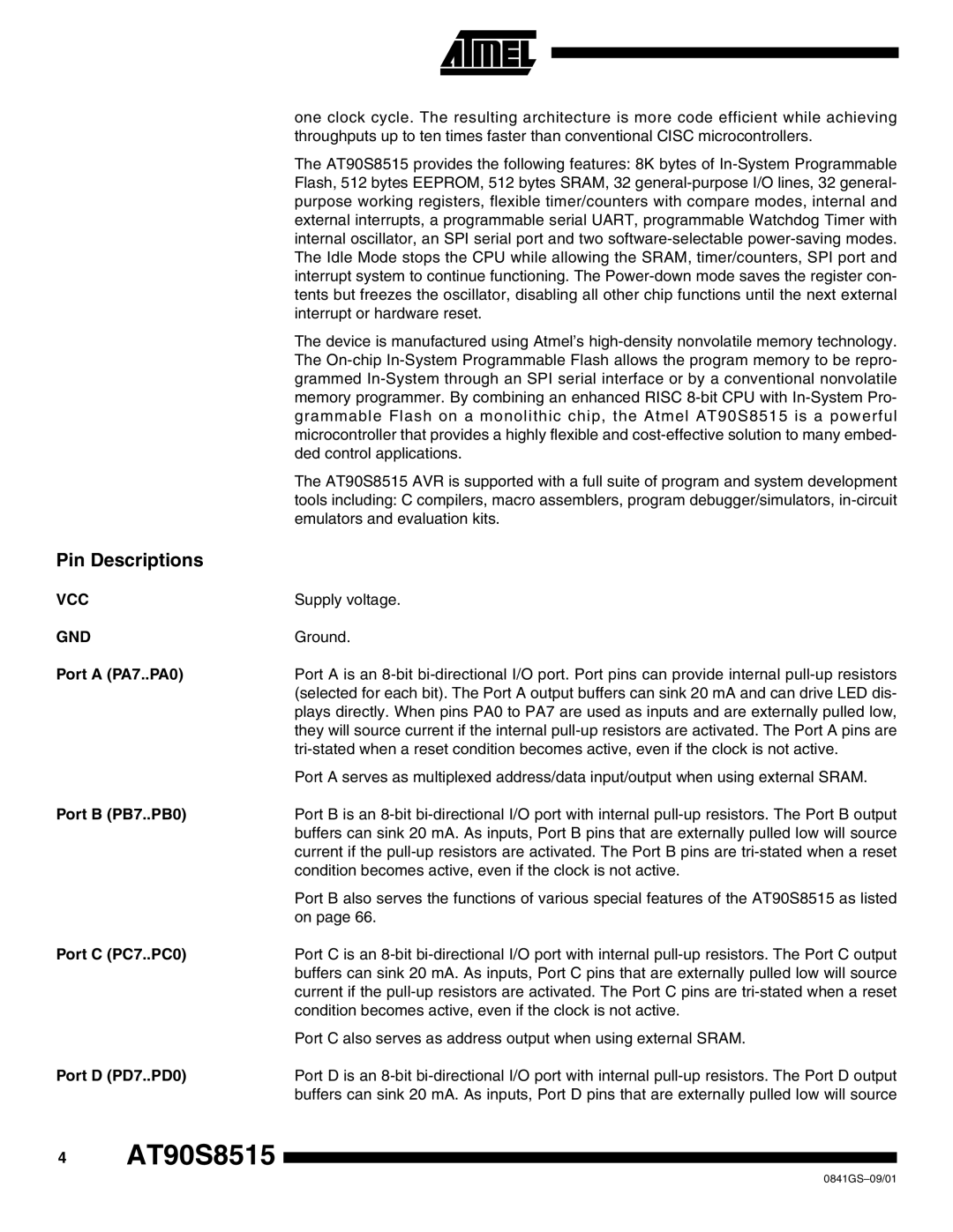
The Atmel AT90S8515-4 is a popular 8-bit microcontroller that belongs to the AVR family, which is widely recognized for its efficient and powerful performance in various embedded applications. It was designed primarily for use in control, automation, and consumer electronic devices, making it one of the go-to choices for developers seeking versatility and reliability.One of the primary features of the AT90S8515-4 is its 8-bit RISC architecture, which allows for a high level of efficiency in instruction execution. This architecture supports a rich set of 32 general-purpose registers, which enable fast data manipulation and make the microcontroller capable of handling complex computations with minimal overhead. The microcontroller operates at clock speeds of up to 4 MHz, providing sufficient speed for a wide range of applications without incurring excessive power consumption.
The AT90S8515-4 comes with a substantial 8 KB of programmable Flash memory, allowing developers to store and execute code efficiently. Additionally, it includes 512 bytes of SRAM, which is essential for temporary data storage during program execution. The microcontroller also features 512 bytes of EEPROM, which is particularly useful for applications requiring non-volatile memory to retain settings or important data even after power loss.
Another important characteristic of the AT90S8515-4 is its versatile I/O capabilities. The microcontroller is equipped with 32 general-purpose I/O pins that can be configured for various digital input or output functions. Moreover, it features an integrated 10-bit Analog-to-Digital Converter (ADC) that simplifies the process of interfacing with analog sensors, enabling precise signal processing.
The AT90S8515-4 also incorporates several built-in communication interfaces, including USART for serial communication, which opens up possibilities for connecting to other devices and systems. This makes it ideal for applications such as data logging, sensor networks, and remote control systems.
In terms of power management, the AT90S8515-4 is designed to operate in various power modes, including a power-saving sleep mode, which prolongs battery life in portable and remote applications.
In summary, the Atmel AT90S8515-4 microcontroller offers a robust blend of features, including a high-performance RISC architecture, ample Flash and EEPROM memory, versatile I/O options, and integrated communication capabilities, making it a suitable choice for developers looking to create efficient and reliable embedded systems.

