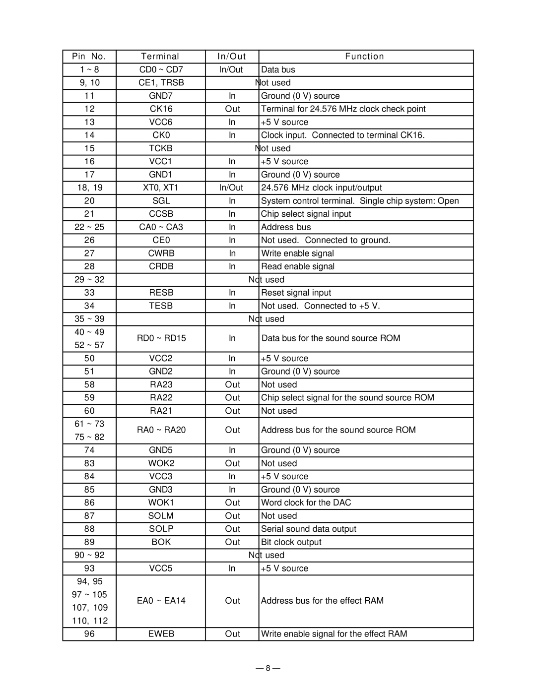
WK-1500 specifications
The Casio WK-1500 is a versatile and user-friendly keyboard designed for aspiring musicians and experienced players alike. Part of Casio’s renowned line of portable keyboards, the WK-1500 combines advanced features with a compact design, making it a suitable choice for both home practice and live performances.At the heart of the WK-1500 is its impressive sound engine, which boasts an extensive library of sounds. With over 600 built-in tones, including a variety of acoustic and electronic instruments, players can easily find the perfect voice for any musical genre. The keyboard also features over 180 rhythms, allowing users to explore a broader musical landscape and enhance their compositions with supportive accompaniments.
One of the standout features of the WK-1500 is its 76 full-size touch-sensitive keys. This is particularly beneficial for pianists, as the touch sensitivity provides a more responsive playing experience. Players can express dynamics and nuances in their performances, enriching their musical interpretations.
The WK-1500 is also equipped with a powerful performance tool known as the "Advanced Synthesizer." This technology allows users to create and modify sounds in real-time, providing endless creative possibilities. Additionally, the keyboard includes a built-in arpeggiator that offers various patterns and styles, further expanding the creative potential.
For those who enjoy composing and recording, the WK-1500 offers built-in song storage with the ability to save and play back original compositions. Users can also connect the keyboard to a computer via USB, making it easy to transfer MIDI data or use the keyboard in conjunction with digital audio workstations.
Another notable characteristic of the WK-1500 is its durability and portability. Weighing in at just under 10 pounds, it is lightweight enough to transport easily. The keyboard also comes with a robust stand and a power adapter, ensuring that musicians can play wherever they go.
In conclusion, the Casio WK-1500 is a feature-packed keyboard that caters to the needs of a wide range of musicians. With its extensive sound library, touch-sensitive keys, advanced synthesizer capabilities, and portability, the WK-1500 stands out as an excellent choice for both learning and performing, ensuring it remains a popular option in the world of portable keyboards. This combination of features, technology, and user-friendly design makes it a valuable instrument for music enthusiasts of all levels.

