Schematic Diagrams

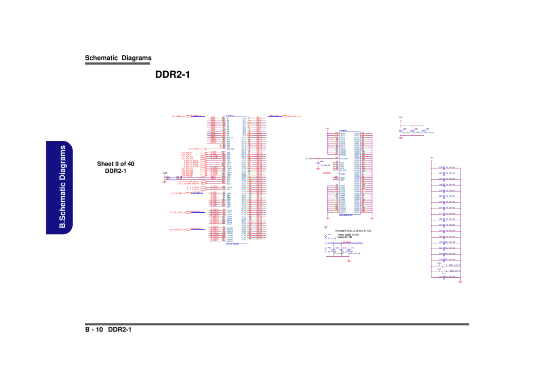
DDR2-1

6,10 MAA[0:13]

MAA[0:13]


MAA0


MAA1


MAA2


MAA3


MAA4


MAA5

102


JDIMM1A


5

MD_0


MD_[0:63]

MD_[0:63] 6,10


A0

DQ0


101


7

MD_1


A1

DQ1


100


17

MD_2


A2

DQ2


99


19

MD_3


A3

DQ3


98


4

MD_4


A4

DQ4


97


6

MD_5


1.8V

B.Schematic Diagrams

Sheet 9 of 40

DDR2-1


MAA6


MAA7


MAA8


MAA9


MAA10


MAA11


MAA12


MAA13


6,10 M_BA2


M_BA0

6,10

M_BA0

M_BA1

6,10

M_BA1

M_CS2#

6,10

M_CS2#

M_CS3#

6,10

M_CS3#


2M_CLK_DDR2

2M_CLK_DDR#2

2M_CLK_DDR3


2 M_CLK_DDR#3


M_CKE2


6,10 M_CKE2


M_CKE3


6,10 M_CKE3


M_CAS#


6,10 M_CAS#


3.3VS


M_RAS#


6,10 M_RAS#


M_WE#


6,10 M_WE#


R65


10K_06


Z0901


R72


10K_06


Z0902


2,10,11,16 SMB_SBCLK


2,10,11,16 SMB_SBDATA


M_ODT2


6,10 M_ODT2


M_ODT3


6,10 M_ODT3


6,10 M_DM[0..7]


M_DM[0..7]


M_DM0


M_DM1


M_DM2


M_DM3


M_DM4


M_DM5


M_DM6


M_DM7


M_DQS+[0..7]


M_DQS+0

6,10

M_DQS+[0..7]


M_DQS+1


M_DQS+2


M_DQS+3


M_DQS+4


M_DQS+5


M_DQS+6


M_DQS+7


M_DQS-[0..7]


M_DQS-0

6,10

M_DQS-[0..7]


M_DQS-1


M_DQS-2


M_DQS-3

M_DQS-4

M_DQS-5

M_DQS-6

M_DQS-7


A5

DQ5


94


14

MD_6


A6

DQ6


92


16

MD_7


A7

DQ7


93


23

MD_8


A8

DQ8


91


25

MD_9


A9

DQ9


105


35

MD_10


A10/AP

DQ10


90


37

MD_11


A11

DQ11


89


20

MD_12


A12

DQ12


116


22

MD_13


A13

DQ13


86


36

MD_14


A14

DQ14


84


38

MD_15


A15

DQ15


85


43

MD_16


A16_BA2

DQ16


45

MD_17


DQ17


107


BA0


55

MD_18


106


DQ18


57

MD_19


BA1

DQ19


110


44

MD_20


S0#

DQ20


115


46

MD_21

3.3VS

30


S1#

DQ21


56

MD_22


CK0

DQ22


32


58

MD_23


CK0#

DQ23


164


61

MD_24


166


CK1

DQ24


63

MD_25


CK1#

DQ25


79


73

MD_26


CKE0

DQ26


80


75

MD_27


CKE1

DQ27


113


62

MD_28


CAS#

DQ28


108


64

MD_29


RAS#

DQ29


109


74

MD_30


WE#

DQ30


198


76

MD_31


SA0

DQ31


200


123

MD_32


SA1

DQ32


197


125

MD_33


SCL

DQ33


195


135

MD_34


SDA

DQ34


137

MD_35


DQ35


114


124

MD_36


ODT0

DQ36


119


126

MD_37


ODT1

DQ37


134

MD_38


DQ38


10


DM0


136

MD_39


DQ39


26


141

MD_40


DM1

DQ40


52


143

MD_41


DM2

DQ41


67


151

MD_42


DM3

DQ42


130


153

MD_43


DM4

DQ43


147


140

MD_44


DM5

DQ44


170


142

MD_45


DM6

DQ45


185


152

MD_46


DM7

DQ46


154

MD_47


DQ47


13


DQS0


157

MD_48


DQ48


31


159

MD_49


DQS1

DQ49


51


173

MD_50


DQS2

DQ50


70


175

MD_51


DQS3

DQ51


131


158

MD_52


DQS4

DQ52


148


160

MD_53


DQS5

DQ53


169


174

MD_54


DQS6

DQ54


188


176

MD_55


DQS7

DQ55


179

MD_56


DQ56


11


DQS0#


181

MD_57


DQ57


29


189

MD_58


DQS1#

DQ58


49


191

MD_59


DQS2#

DQ59


68


180

MD_60


DQS3#

DQ60


129


182

MD_61


DQS4#

DQ61


146


192

MD_62


DQS5#

DQ62


167


194

MD_63


DQS6#

DQ63


186


DQS7#


CA0145-200N02


1.8V


JDIMM1B


112


18


VDD1

VSS16


111

24


VDD2

VSS17


117

41


VDD3

VSS18


96

53


VDD4

VSS19


95

42


VDD5

VSS20


118

54


VDD6

VSS21


81

59


VDD7

VSS22


82

65


VDD8

VSS23


87

60


VDD9

VSS24


103

66


VDD10

VSS25


88

127


VDD11

VSS26


104

139


VDD12

VSS27


128


VSS28


199


145


VDDSPD

VSS29

165


VSS30

C69

83


171

NC1

VSS31


120

172

.1U_50V_06

50

NC2

VSS32

177

NC3

VSS33


69

187


NC4

VSS34


163

178


NCTEST

VSS35

190


VSS36

SDREFD

1


9

VREF

VSS37


21


201


VSS38

33


GND0

VSS39


202

155


GND1

VSS40


34


VSS41

132


VSS42


47


144


VSS1

VSS43


133

156


VSS2

VSS44


183

168


VSS3

VSS45


77

2


VSS4

VSS46


12

3


VSS5

VSS47


48

15


VSS6

VSS48


184

27


VSS7

VSS49


78

39


VSS8

VSS50


71

149


VSS9

VSS51


72

161


VSS10

VSS52


121

28


VSS11

VSS53


122

40


VSS12

VSS54


196

138


VSS13

VSS55


193

150


VSS14

VSS56


8

162


VSS15

VSS57


CA0145-200N02


1.8V

DDRVREF GEN. & DECOUPLING

R71 Trace Width 12 Mil

75_1%_06 Space 20 Mil

SDREFD

R70 C68 C70 C71

75_1%_06 2.2U_6.3V_06

.1U_16V_04 2.2U_6.3V_06

C66 C33 C34

.1U_16V_04 .1U_16V_04 .1U_16V_04

1.8V

C35 .1U_16V_04

C67 .1U_16V_04

C83 .1U_16V_04

C36 .1U_16V_04

C32 .1U_16V_04

C65 .1U_16V_04

C30 .1U_16V_06

C78 .1U_16V_06

C77 .1U_16V_06

C76 .1U_16V_06

C75 .1U_16V_06

C63 .1U_16V_06

C64 .1U_16V_06

C72 10U_10V_08

C81 10U_10V_08

C49 10U_10V_08

C29 10U_10V_08

C43

1 2 330U_6.3V_D

+


C44


2 *330U_6.3V_D

1


+


C48


10U_10V_08


B - 10 DDR2-1

Page 62
Image 62
Clevo M665SE manual Sheet 9 DDR2-1

M665SE specifications

The Clevo M665SE is a versatile gaming laptop designed to meet the needs of both gamers and professionals seeking robust performance and reliability. With its powerful specifications and innovative technology, it stands out as an excellent choice for a wide range of applications.

At the heart of the Clevo M665SE is the latest generation Intel Core processor, which delivers exceptional performance and efficiency. This processor ensures that users can run demanding applications and games seamlessly, with speeds and responsiveness that significantly enhance productivity and gaming experiences. The laptop can be configured with higher-end CPUs, giving users a choice based on their performance requirements.

Graphics performance is equally impressive, with options for dedicated NVIDIA GeForce graphics cards. This allows for smooth rendering of high-definition graphics and supports demanding games and design software. The M665SE can easily handle the latest titles, providing an immersive gaming experience with vibrant visuals and fluid frame rates.

Another key feature of the Clevo M665SE is its expansive storage and memory options. With support for multiple SSDs and HDDs, users can enjoy high-speed data access alongside substantial storage capacity. This flexibility allows for quick boot times and efficient file management, catering to those who require large volumes of storage for games, media, or professional applications.

The M665SE also incorporates advanced cooling technology, ensuring that the laptop remains stable and performs optimally even during intense gaming sessions. Its thoughtful design around ventilation helps prevent overheating, extending the lifespan of the components while maintaining peak performance.

Display quality is another highlight of the Clevo M665SE. It typically features a high-resolution display with excellent color accuracy and wide viewing angles, making it suitable for multimedia consumption and professional graphic work. The addition of features like anti-glare technology enhances usability in diverse lighting conditions.

Connectivity options are plentiful on the M665SE, with various ports that support USB, HDMI, and Ethernet connections. This ensures compatibility with a range of peripherals and external displays, allowing for a flexible setup whether at home or on the go.

Overall, the Clevo M665SE combines powerful performance, high-quality graphics, and impressive flexibility, making it an ideal choice for gamers and professionals who require a reliable and feature-rich laptop. Its combination of cutting-edge technology and thoughtful design makes it a standout option in the competitive laptop market.