4 Signal Description
4 Signal Description
4.1Graphic Signal Description
Based on the different available graphic interfaces offered by the different chipsets from silicon vendors including Intel, ATI, VIA, etc., there is a need for optional assignment in addition to the ones already defined by PICMG in the COM.0 specification. These will allow for ease when integrating upcoming new graphic interfaces while still assuring compatibility of COM Express™ compliant modules and carrier boards.
Graphic signals are defined on Row C and Row D.
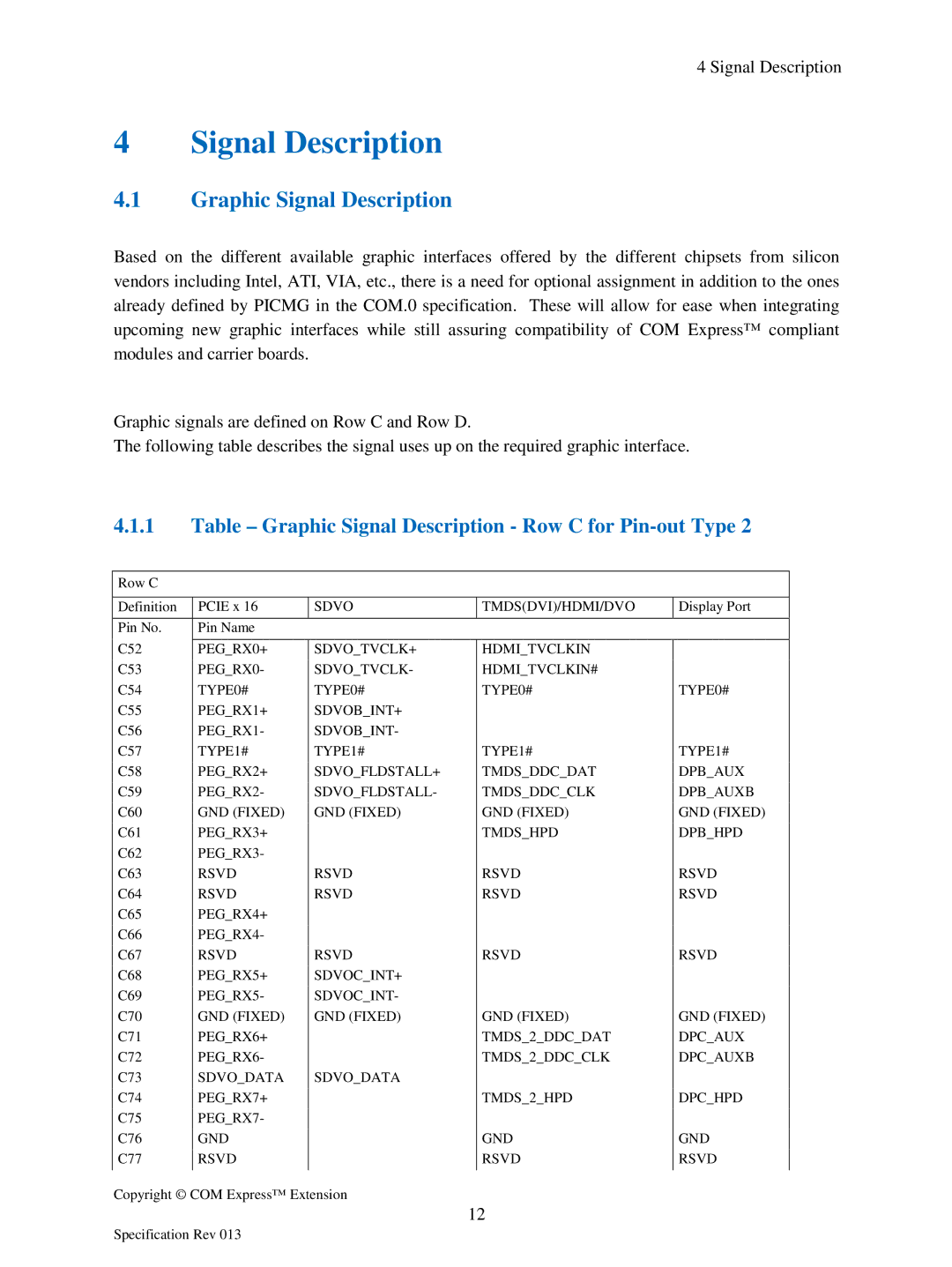
The following table describes the signal uses up on the required graphic interface.
4.1.1Table – Graphic Signal Description - Row C for Pin- out Type 2
Row C
Definition | PCIE x 16 | SDVO | TMDS(DVI)/HDMI/DVO | Display Port |
|
|
|
|
|
Pin No. | Pin Name |
|
|
|
|
|
|
|
|
C52 | PEG_RX0+ | SDVO_TVCLK+ | HDMI_TVCLKIN |
|
C53 | PEG_RX0- | SDVO_TVCLK- | HDMI_TVCLKIN# |
|
C54 | TYPE0# | TYPE0# | TYPE0# | TYPE0# |
C55 | PEG_RX1+ | SDVOB_INT+ |
|
|
C56 | PEG_RX1- | SDVOB_INT- |
|
|
C57 | TYPE1# | TYPE1# | TYPE1# | TYPE1# |
C58 | PEG_RX2+ | SDVO_FLDSTALL+ | TMDS_DDC_DAT | DPB_AUX |
C59 | PEG_RX2- | SDVO_FLDSTALL- | TMDS_DDC_CLK | DPB_AUXB |
C60 | GND (FIXED) | GND (FIXED) | GND (FIXED) | GND (FIXED) |
C61 | PEG_RX3+ |
| TMDS_HPD | DPB_HPD |
C62 | PEG_RX3- |
|
|
|
C63 | RSVD | RSVD | RSVD | RSVD |
C64 | RSVD | RSVD | RSVD | RSVD |
C65 | PEG_RX4+ |
|
|
|
C66 | PEG_RX4- |
|
|
|
C67 | RSVD | RSVD | RSVD | RSVD |
C68 | PEG_RX5+ | SDVOC_INT+ |
|
|
C69 | PEG_RX5- | SDVOC_INT- |
|
|
C70 | GND (FIXED) | GND (FIXED) | GND (FIXED) | GND (FIXED) |
C71 | PEG_RX6+ |
| TMDS_2_DDC_DAT | DPC_AUX |
C72 | PEG_RX6- |
| TMDS_2_DDC_CLK | DPC_AUXB |
C73 | SDVO_DATA | SDVO_DATA |
|
|
C74 | PEG_RX7+ |
| TMDS_2_HPD | DPC_HPD |
C75 | PEG_RX7- |
|
|
|
C76 | GND |
| GND | GND |
C77 | RSVD |
| RSVD | RSVD |
|
|
|
|
|
Copyright © COM Express™ Extension
12
Specification Rev 013
