5 Hardware extensions
5.2.1Alternative GPIO use for SDIO Interface
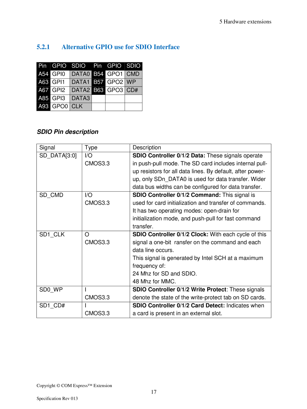
Pin A54 A63 A67 A85 A93
GPIO SDIO Pin GPIO SDIO GPI0 DATA0 B54 GPO1 CMD GPI1 DATA1 B57 GPO2 WP GPI2 DATA2 B63 GPO3 CD# GPI3 DATA3
GPO0 CLK
SDIO Pin description
Signal | Type | Description |
|
|
|
SD_DATA[3:0] | I/O | SDIO Controller 0/1/2 Data: These signals operate |
| CMOS3.3 | in |
|
| up resistors for all data lines. By default, after power- |
|
| up, only SDn_DATA0 is used for data transfer. Wider |
|
| data bus widths can be configured for data transfer. |
|
|
|
SD_CMD | I/O | SDIO Controller 0/1/2 Command: This signal is |
| CMOS3.3 | used for card initialization and transfer of commands. |
|
| It has two operating modes: |
|
| initialization mode, and |
|
| transfer. |
|
|
|
SD1_CLK | O | SDIO Controller 0/1/2 Clock: With each cycle of this |
| CMOS3.3 | signal a |
|
| data line occurs. |
|
| This signal is generated by Intel SCH at a maximum |
|
| frequency of: |
|
| 24 Mhz for SD and SDIO. |
|
| 48 Mhz for MMC. |
|
|
|
SD0_WP | I | SDIO Controller 0/1/2 Write Protect: These signals |
| CMOS3.3 | denote the state of the |
|
|
|
SD1_CD# | I | SDIO Controller 0/1/2 Card Detect: Indicates when |
| CMOS3.3 | a card is present in an external slot. |
|
|
|
Copyright © COM Express™ Extension
17
Specification Rev 013