EZ-USB FX2™ PCB Design Recommendations

AN1196

Introduction

This application note presents recommendations for design- ing with the Cypress Semiconductor EZ-USB FX2™ compo- nent. Techniques for high-speed design should be applied to circuits using the EZ-USB FX2. Due to the packaging and high performance characteristics of the EZ-USB FX2, consid- eration of the PCB thermal design is required.

EZ-USB FX2 Package Description

The CY7C68013-56LFC EZ-USB FX2 component is pack- aged as a 56-pad, 8-mm by 8-mm, 1-mm high, QFN (Quad Flatpack No leads) package. Please refer to the latest CY7C68013 EZ-USB FX2 USB Microcontroller High-speed USB Peripheral Controller data sheet for the detailed pack- age drawing. The data sheet is Cypress specification 38- 08012.

CY4611 EZ-USB FX2 USB to ATA Reference Design

A complete design using the Cypress CY7C68013 EZ-USB FX2 is available. The design implements the recommenda- tions of this application note. It may be useful for the reader to download the CY4611 Reference Design Files from the Cypress Support page for Reference Designs.

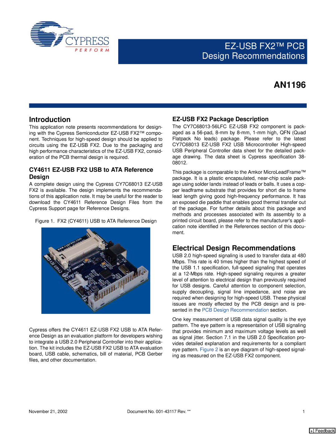
Figure 1. FX2 (CY4611) USB to ATA Reference Design

Cypress offers the CY4611 EZ-USB FX2 USB to ATA Refer- ence Design as an evaluation platform for developers wishing to integrate a USB 2.0 Peripheral Controller into their applica- tion. The kit includes the EZ-USB FX2 USB to ATA evaluation board, USB cable, schematics, bill of material, PCB Gerber files, and other documentation.

This package is comparable to the Amkor MicroLeadFrame™ package. It is a plastic encapsulated, near-chip scale pack- age using solder lands instead of leads or balls. It uses a cop- per leadframe substrate that provides for short die to frame lead length giving good high-frequency performance. It has an exposed die paddle that enables good thermal transfer out of the package. For further details about this package and methods and processes associated with its assembly to a printed circuit board, please refer to the manufacturer's appli- cation note identified in the References section of this docu- ment.

Electrical Design Recommendations

USB 2.0 high-speed signaling is used to transfer data at 480 Mbps. This rate is 40 times higher than the highest speed of the USB 1.1 specification, full-speed signaling that operates at a 12-Mbps rate. High-speed signaling requires a greater level of attention to electrical design than previously required for USB designs. Careful attention to component selection, supply decoupling, signal line impedance, and noise are required when designing for high-speed USB. These physical issues are mostly effected by the PCB design and is pre- sented in the PCB Design Recommendation section.

One key measurement of USB data signal quality is the eye pattern. The eye pattern is a representation of USB signaling that provides minimum and maximum voltage levels as well as signal jitter. Section 7.1 in the USB 2.0 Specification pro- vides detailed explanation and requirements for a compliant eye pattern. Figure 2 is an eye diagram of high-speed signal- ing as measured on the EZ-USB FX2 component.

November 21, 2002

Document No. 001-43117 Rev. **

1

[+] Feedback

Page 1
Image 1
Cypress EZ-USB FX2 PCB, AN1196 manual Introduction, Electrical Design Recommendations, EZ-USB FX2 Package Description

AN1196, EZ-USB FX2 PCB specifications

The Cypress EZ-USB FX2 is a high-speed USB microcontroller that serves as a versatile platform for connecting various devices to a USB interface. Designed for applications requiring a seamless and efficient USB communication system, the FX2 is widely used in data acquisition, imaging, and consumer electronics. The AN1196 application note is a pivotal resource that provides comprehensive guidance on utilizing the FX2 for developing USB peripherals.

One of the standout features of the Cypress EZ-USB FX2 is its ability to support high-speed USB 2.0 data transfer rates of up to 480 Mbps. This high bandwidth allows it to handle large data flows efficiently, making it suitable for applications such as high-resolution imaging or real-time data streaming. The FX2 architecture is designed to facilitate easy integration with various types of peripherals, allowing developers to create devices that communicate effectively over USB.

The FX2 microcontroller is built on an 8051 core, which is known for its low power consumption and efficient processing capabilities. With 64 Kbytes of on-chip RAM and 8 Kbytes of ROM, it provides ample resources for firmware and data storage. The built-in FIFO buffer is a significant advantage, enabling smooth data transfers between the USB interface and the device, thus reducing the complexity typically associated with USB communication.

A range of development tools and libraries simplifies the programming of the FX2 device. The EZ-USB developer toolkit includes libraries for quick integration and support for various development environments. This toolkit allows engineers to focus on higher-level application designs rather than getting bogged down in the intricacies of USB protocol implementation.

In terms of power management, the FX2 supports various modes to minimize power consumption during idle periods. This feature is particularly useful in battery-powered applications or scenarios where energy efficiency is crucial. Moreover, the device offers flexibility with its GPIO pins, allowing developers to configure them for different functionalities such as I2C, SPI, or GPIO operations, expanding its utility across various applications.

Overall, the Cypress EZ-USB FX2, together with the guidance provided in the AN1196 application note, equips developers with the resources needed to build robust USB solutions that cater to diverse market needs. Its combination of high-speed performance, low-power operation, and flexibility makes it a popular choice in the embedded systems community.