Undershoot Effect in RTC Circuit of 0.25μ nvSRAM
AN49947
Associated Part Family: CY14BXXXK/STK17TX8
GET FREE SAMPLES HERE
Application Note Abstract
This application note describes the undershoot effect in the RTC circuit of the 256K and 1M nvSRAM in 0.25μ technology. The part numbers affected are CY14B256K/STK17T88 and CY14B101K/STK17TA8.
Introduction
Under certain noise conditions, the Real Time Clock (RTC) circuit of CY14BXXXK/STK17TX8 can be disturbed to the point that the oscillator circuit stops.
Undershoot in Application
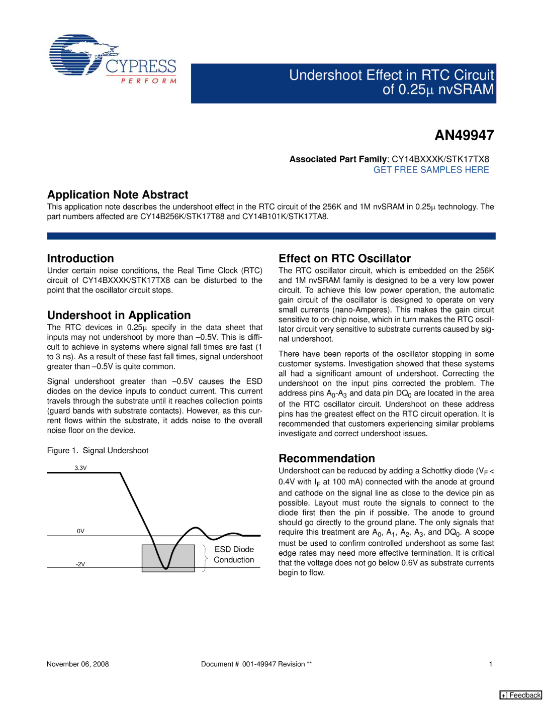
The RTC devices in 0.25μ specify in the data sheet that inputs may not undershoot by more than
Signal undershoot greater than
Figure 1. Signal Undershoot
3.3V
0V
| ESD Diode |
| EDS DIODE |
CONDUCTIONConduction | |
|
Effect on RTC Oscillator
The RTC oscillator circuit, which is embedded on the 256K and 1M nvSRAM family is designed to be a very low power circuit. To achieve this low power operation, the automatic gain circuit of the oscillator is designed to operate on very small currents
There have been reports of the oscillator stopping in some customer systems. Investigation showed that these systems all had a significant amount of undershoot. Correcting the undershoot on the input pins corrected the problem. The address pins
Recommendation
Undershoot can be reduced by adding a Schottky diode (VF < 0.4V with IF at 100 mA) connected with the anode at ground and cathode on the signal line as close to the device pin as possible. Layout must route the signals to connect to the diode first then the pin if possible. The anode to ground should go directly to the ground plane. The only signals that require this treatment are A0, A1, A2, A3, and DQ0. A scope must be used to confirm controlled undershoot as some fast edge rates may need more effective termination. It is critical that the voltage does not go below 0.6V as substrate currents begin to flow.
November 06, 2008 | Document # | 1 |
[+] Feedback