CY7C1316JV18, CY7C1916JV18
CY7C1318JV18, CY7C1320JV18
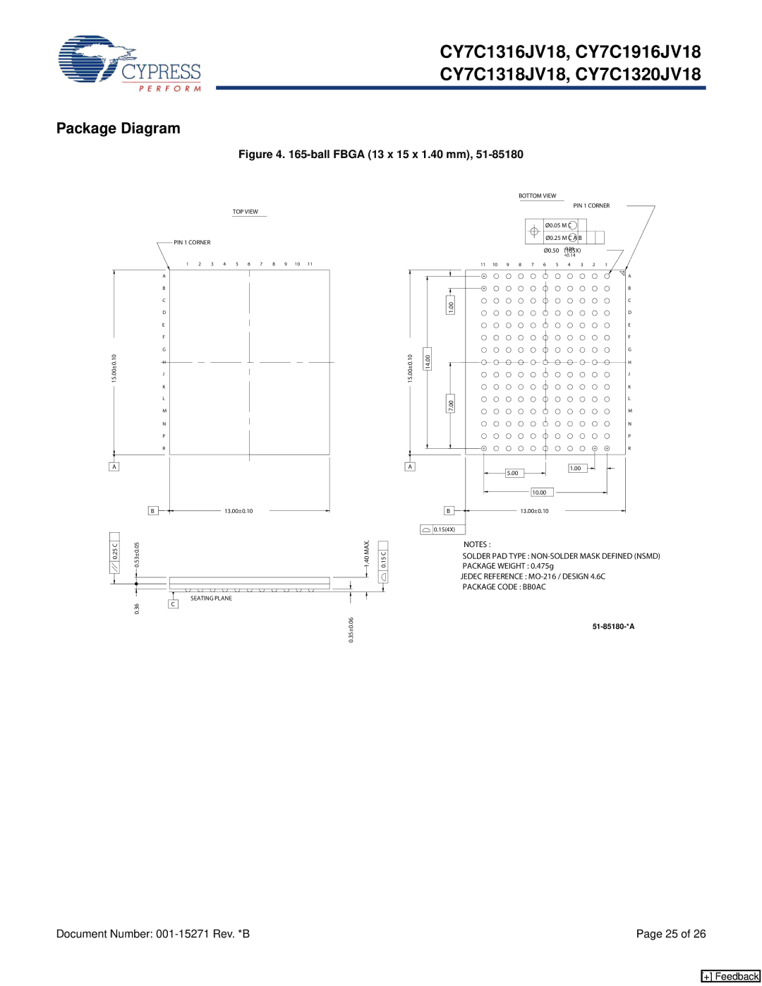
Package Diagram
Figure 4. 165-ball FBGA (13 x 15 x 1.40 mm), 51-85180
15.00±0.10
A
TOP VIEW
PIN 1 CORNER
1 | 2 | 3 | 4 | 5 | 6 | 7 | 8 | 9 | 10 | 11 |
A
B
C
D
E
F
G
H
J
K
L
M
N
P
R
1.00
15.00±0.10 | 14.00 |
|
7.00
A
BOTTOM VIEW
PIN 1 CORNER
Ø0.05 M C
Ø0.25 M C A B
Ø0.50 (165X)
+0.14
11 | 10 | 9 | 8 | 7 | 6 | 5 | 4 | 3 | 2 | 1 |
A
B
C
D
E
F
G
H
J
K
L
M
N
P
R
1.00 |
5.00 |
10.00 |
0.25 C
| B |
0.53±0.05 |
|
0.36 | C |
|
13.00±0.10
|
| 1.40MAX. |
|
|
|
|
|
|
|
| |||
| 0.15C | |||||
|
|
|
|
|
|
|
|
|
|
|
|
|
|
|
|
|
|
|
|
|
SEATING PLANE
0.35±0.06
B ![]()
![]()
 13.00±0.10
0.15(4X)
NOTES :
SOLDER PAD TYPE :
PACKAGE WEIGHT : 0.475g
JEDEC REFERENCE :
Document Number: | Page 25 of 26 |
[+] Feedback