|
|
|
|
|
|
|
|
|
|
|
|
|
|
|
|
|
|
|
|
|
|
|
|
|
|
|
|
|
|
|
|
|
|
|
|
|
|
|
|
|
|
|
|
|
|
|
|
|
|
|
|
|
|
| CY7C1316JV18, CY7C1916JV18 | |||||||||||||||||||
|
|
|
|
|
|
|
|
|
|
|
|
|
|
|
|
|
|
|
|
|
|
|
|
|
|
|
|
|
|
|
|
|
|
|
|
|
|
|
|
|
|
|
|
|
|
|
|
|
|
|
|
|
|
| CY7C1318JV18, CY7C1320JV18 | |||||||||||||||||||
|
|
|
|
|
|
|
|
|
|
|
|
|
|
|
|
|
|
|
|
|
|
|
|
|
|
|
|
|
|
|
|
|
|
|
|
|
|
|
|
|
|
|
|
|
|
|
|
|
|
|
|
|
|
|
|
|
|
|
|
|
|
|
|
|
|
|
|
|
|
|
|
|
| |
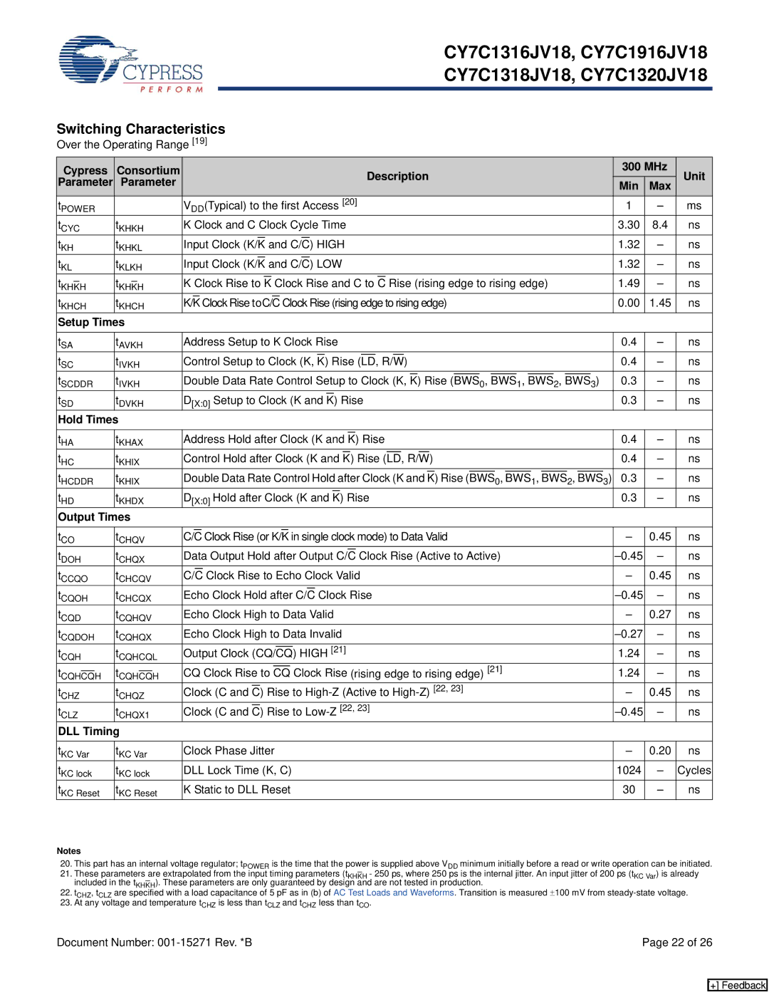
Switching Characteristics |
|
|
| |||||||||||||||||||||||||||||||||||||||||||||||||||||||||||||||||||||||
Over the Operating Range [19] |
|
|
| |||||||||||||||||||||||||||||||||||||||||||||||||||||||||||||||||||||||
| Cypress | Consortium |
|
|
|
|
|
|
|
|
|
|
|
|
|
|
|
|
|
|
|
|
|
|
|
|
|
|
|
|
|
|
|
|
|
|
|
|
|
| Description | 300 MHz | Unit | |||||||||||||||||||||||||||||||
Parameter | Parameter |
|
|
|
|
|
|
|
|
|
|
|
|
|
|
|
|
|
|
|
|
|
|
|
|
|
|
|
|
|
|
|
|
|
|
|
|
|
| Min | Max | |||||||||||||||||||||||||||||||||
|
|
|
|
|
|
|
|
|
|
|
|
|
|
|
|
|
|
|
|
|
|
|
|
|
|
|
|
|
|
|
|
|
|
|
|
|
|
|
|
|
|
|
|
|
|
|
|
|
|
|
|
|
|
|
|
|
|
|
|
|
|
|
|
|
|
|
| |||||||
|
|
|
|
|
|
|
|
|
|
|
|
|
|
|
|
|
|
|
|
|
|
|
|
|
|
|
|
|
|
|
|
|
|
|
|
|
|
|
|
|
|
|
|
|
|
|
|
|
|
|
|
|
|
|
|
|
|
|
|
|
|
|
|
|
|
|
|
|
|
|
|
| ||
t | POWER |
|
| V (Typical) to the first Access [20] | 1 | – | ms | |||||||||||||||||||||||||||||||||||||||||||||||||||||||||||||||||||
|
|
| DD |
|
|
| ||||||||||||||||||||||||||||||||||||||||||||||||||||||||||||||||||||
tCYC | tKHKH | K Clock and C Clock Cycle Time | 3.30 | 8.4 | ns | |||||||||||||||||||||||||||||||||||||||||||||||||||||||||||||||||||||
tKH | tKHKL |
|
|
|
|
|
|
|
|
|
|
|
|
|
|
|
|
|
|
|
|
|
|
|
|
|
|
|
|
|
|
|
|
|
|
|
|
|
|
|
|
|
|
|
|
|
|
|
|
|
|
|
|
|
|
|
|
|
|
|
|
|
|
|
|
|
|
|
|
|
| |||
Input Clock (K/K | and C/C) HIGH | 1.32 | – | ns | ||||||||||||||||||||||||||||||||||||||||||||||||||||||||||||||||||||||
tKL | tKLKH |
|
|
|
|
|
|
|
|
|
|
|
|
|
|
|
|
|
|
|
|
|
|
|
|
|
|
|
|
|
|
|
|
|
|
|
|
|
|
|
|
|
|
|
|
|
|
|
|
|
|
|
|
|
|
|
|
|
|
|
|
|
|
|
|
|
|
|
|
|
| |||
Input Clock (K/K | and C/C) LOW | 1.32 | – | ns | ||||||||||||||||||||||||||||||||||||||||||||||||||||||||||||||||||||||
tKHKH | tKHKH | K Clock Rise to |
|
|
|
| Clock Rise and C to |
|
| Rise (rising edge to rising edge) | 1.49 | – | ns | |||||||||||||||||||||||||||||||||||||||||||||||||||||||||||||
K | C | |||||||||||||||||||||||||||||||||||||||||||||||||||||||||||||||||||||||||
tKHCH | tKHCH |
|
|
|
|
|
|
|
|
|
|
|
|
|
|
|
|
|
|
|
|
|
|
|
|
|
|
|
|
|
|
|
|
|
|
|
|
|
|
|
|
|
|
|
|
|
|
|
|
|
|
|
|
|
|
|
|
|
|
|
|
|
|
|
|
|
|
|
|
|
| |||
K/K |
| Clock Rise to C/C Clock Rise (rising edge to rising edge) | 0.00 | 1.45 | ns | |||||||||||||||||||||||||||||||||||||||||||||||||||||||||||||||||||||
Setup Times |
|
|
|
|
|
|
|
|
|
|
|
|
|
|
|
|
|
|
|
|
|
|
|
|
|
|
|
|
|
|
|
|
|
|
|
|
|
|
|
|
|
|
|
|
|
|
|
|
|
|
|
|
|
|
|
|
|
|
|
|
|
|
|
|
|
|
|
|
|
| ||||
|
|
|
|
|
| |||||||||||||||||||||||||||||||||||||||||||||||||||||||||||||||||||||
tSA | tAVKH | Address Setup to K Clock Rise | 0.4 | – | ns | |||||||||||||||||||||||||||||||||||||||||||||||||||||||||||||||||||||
tSC | tIVKH | Control Setup to Clock (K, |
|
|
|
|
|
|
|
|
|
|
|
|
|
|
|
|
|
|
|
|
|
|
|
|
|
|
|
|
|
|
|
|
|
|
|
|
|
|
|
| 0.4 | – | ns | |||||||||||||||||||||||||||||
K) Rise (LD, R/W) | ||||||||||||||||||||||||||||||||||||||||||||||||||||||||||||||||||||||||||
tSCDDR | tIVKH | Double Data Rate Control Setup to Clock (K, |
|
|
|
|
|
|
|
|
|
|
|
|
|
|
|
|
|
|
|
|
| 0.3 | – | ns | ||||||||||||||||||||||||||||||||||||||||||||||||
K) Rise (BWS0, BWS1, BWS2, BWS3) | ||||||||||||||||||||||||||||||||||||||||||||||||||||||||||||||||||||||||||
tSD | tDVKH | D[X:0] Setup to Clock (K and |
|
|
|
|
|
|
|
|
|
|
|
|
|
|
|
|
|
|
|
|
|
|
|
|
|
|
|
|
|
|
|
|
|
|
|
|
|
| 0.3 | – | ns | |||||||||||||||||||||||||||||||
K) Rise | ||||||||||||||||||||||||||||||||||||||||||||||||||||||||||||||||||||||||||
Hold Times |
|
|
|
|
|
|
|
|
|
|
|
|
|
|
|
|
|
|
|
|
|
|
|
|
|
|
|
|
|
|
|
|
|
|
|
|
|
|
|
|
|
|
|
|
|
|
|
|
|
|
|
|
|
|
|
|
|
|
|
|
|
|
|
|
|
|
|
|
|
| ||||
|
|
|
|
|
|
|
|
|
|
|
|
|
|
|
|
|
|
|
|
|
|
| ||||||||||||||||||||||||||||||||||||||||||||||||||||
tHA | tKHAX | Address Hold after Clock (K and |
|
|
|
|
|
|
|
|
|
|
|
|
|
|
|
|
|
|
|
|
|
|
|
|
|
|
|
|
|
|
|
| 0.4 | – | ns | |||||||||||||||||||||||||||||||||||||
K) Rise | ||||||||||||||||||||||||||||||||||||||||||||||||||||||||||||||||||||||||||
tHC | tKHIX | Control Hold after Clock (K and |
|
|
|
|
|
|
|
|
|
|
|
|
|
|
|
|
|
|
|
|
|
|
|
|
|
|
|
|
|
|
|
|
|
| 0.4 | – | ns | |||||||||||||||||||||||||||||||||||
K) Rise (LD, R/W) | ||||||||||||||||||||||||||||||||||||||||||||||||||||||||||||||||||||||||||
tHCDDR | tKHIX | Double Data Rate Control Hold after Clock (K and |
|
|
|
|
|
|
|
|
|
|
|
|
|
|
|
|
|
|
| 0.3 | – | ns | ||||||||||||||||||||||||||||||||||||||||||||||||||
K) Rise (BWS0, BWS1, BWS2, BWS3) | ||||||||||||||||||||||||||||||||||||||||||||||||||||||||||||||||||||||||||
tHD | tKHDX | D[X:0] Hold after Clock (K and |
|
|
|
|
|
|
|
|
|
|
|
|
|
|
|
|
|
|
|
|
|
|
|
|
|
|
|
|
|
|
|
|
|
|
|
|
| 0.3 | – | ns | ||||||||||||||||||||||||||||||||
K) Rise | ||||||||||||||||||||||||||||||||||||||||||||||||||||||||||||||||||||||||||
Output Times |
|
|
|
|
|
|
|
|
|
|
|
|
|
|
|
|
|
|
|
|
|
|
|
|
|
|
|
|
|
|
|
|
|
|
|
|
|
|
|
|
|
|
|
|
|
|
|
|
|
|
|
|
|
|
|
|
|
|
|
|
|
|
|
|
|
|
|
|
|
| ||||
|
|
|
|
|
|
|
|
|
|
|
|
|
|
|
|
|
|
|
| |||||||||||||||||||||||||||||||||||||||||||||||||||||||
tCO | tCHQV | C/C |
| Clock Rise (or K/K |
| in single clock mode) to Data Valid | – | 0.45 | ns | |||||||||||||||||||||||||||||||||||||||||||||||||||||||||||||||||
tDOH | tCHQX |
|
|
|
|
|
|
|
|
|
|
|
|
|
|
|
|
|
|
|
|
|
|
|
|
|
|
|
|
|
|
|
|
|
|
|
|
| Clock Rise (Active to Active) | – | ns | |||||||||||||||||||||||||||||||||
Data Output Hold after Output C/C | ||||||||||||||||||||||||||||||||||||||||||||||||||||||||||||||||||||||||||
tCCQO | tCHCQV |
|
|
|
|
|
| Clock Rise to Echo Clock Valid | – | 0.45 | ns | |||||||||||||||||||||||||||||||||||||||||||||||||||||||||||||||
C/C | ||||||||||||||||||||||||||||||||||||||||||||||||||||||||||||||||||||||||||
tCQOH | tCHCQX |
|
|
|
|
|
|
|
|
|
|
|
|
|
|
|
|
|
|
|
|
|
|
|
|
|
| Clock Rise | – | ns | ||||||||||||||||||||||||||||||||||||||||||||
Echo Clock Hold after C/C | ||||||||||||||||||||||||||||||||||||||||||||||||||||||||||||||||||||||||||
tCQD | tCQHQV | Echo Clock High to Data Valid | – | 0.27 | ns | |||||||||||||||||||||||||||||||||||||||||||||||||||||||||||||||||||||
tCQDOH | tCQHQX | Echo Clock High to Data Invalid | – | ns | ||||||||||||||||||||||||||||||||||||||||||||||||||||||||||||||||||||||
tCQH | tCQHCQL |
|
|
|
|
|
|
|
|
|
|
|
|
|
|
|
|
|
|
|
|
|
| HIGH [21] | 1.24 | – | ns | |||||||||||||||||||||||||||||||||||||||||||||||
Output Clock (CQ/CQ) | ||||||||||||||||||||||||||||||||||||||||||||||||||||||||||||||||||||||||||
tCQHCQH |
| tCQHCQH |
| CQ Clock Rise to |
|
|
|
|
| Clock Rise (rising edge to rising edge) [21] | 1.24 | – | ns | |||||||||||||||||||||||||||||||||||||||||||||||||||||||||||||
|
| CQ | ||||||||||||||||||||||||||||||||||||||||||||||||||||||||||||||||||||||||
tCHZ | tCHQZ | Clock (C and |
|
|
|
|
|
|
|
|
|
|
|
|
|
|
|
|
|
|
|
|
|
|
|
|
|
|
|
|
|
|
|
|
|
|
|
|
|
|
|
|
|
|
|
|
|
|
|
|
|
|
|
|
|
|
|
|
|
| – | 0.45 | ns | |||||||||||
C) Rise to | ||||||||||||||||||||||||||||||||||||||||||||||||||||||||||||||||||||||||||
tCLZ | tCHQX1 | Clock (C and |
|
|
|
|
|
|
|
|
|
|
|
|
|
|
|
|
|
|
|
|
|
|
|
|
|
|
|
|
|
|
|
|
|
|
|
|
|
|
|
|
|
|
|
|
|
|
|
|
|
|
|
|
|
|
|
|
|
| – | ns | ||||||||||||
C) Rise to | ||||||||||||||||||||||||||||||||||||||||||||||||||||||||||||||||||||||||||
DLL Timing |
|
|
|
|
|
|
|
|
|
|
|
|
|
|
|
|
|
|
|
|
|
|
|
|
|
|
|
|
|
|
|
|
|
|
|
|
|
|
|
|
|
|
|
|
|
|
|
|
|
|
|
|
|
|
|
|
|
|
|
|
|
|
|
|
|
|
|
|
|
| ||||
|
|
|
|
|
| |||||||||||||||||||||||||||||||||||||||||||||||||||||||||||||||||||||
tKC Var | tKC Var | Clock Phase Jitter | – | 0.20 | ns | |||||||||||||||||||||||||||||||||||||||||||||||||||||||||||||||||||||
tKC lock | tKC lock | DLL Lock Time (K, C) | 1024 | – | Cycles | |||||||||||||||||||||||||||||||||||||||||||||||||||||||||||||||||||||
tKC Reset | tKC Reset | K Static to DLL Reset | 30 | – | ns | |||||||||||||||||||||||||||||||||||||||||||||||||||||||||||||||||||||
Notes
20.This part has an internal voltage regulator; tPOWER is the time that the power is supplied above VDD minimum initially before a read or write operation can be initiated.
21.These parameters are extrapolated from the input timing parameters (tKHKH - 250 ps, where 250 ps is the internal jitter. An input jitter of 200 ps (tKC Var) is already included in the tKHKH). These parameters are only guaranteed by design and are not tested in production.
22.tCHZ, tCLZ are specified with a load capacitance of 5 pF as in (b) of AC Test Loads and Waveforms. Transition is measured ±100 mV from
23.At any voltage and temperature tCHZ is less than tCLZ and tCHZ less than tCO.
Document Number: | Page 22 of 26 |
[+] Feedback