CY7C1316JV18, CY7C1916JV18
CY7C1318JV18, CY7C1320JV18
Capacitance
Tested initially and after any design or process change that may affect these parameters.
Parameter | Description | Test Conditions | Max | Unit |
CIN | Input Capacitance | TA = 25°C, f = 1 MHz, VDD = 1.8V, VDDQ = 1.5V | 5 | pF |
CCLK | Clock Input Capacitance |
| 6 | pF |
CO | Output Capacitance |
| 7 | pF |
Thermal Resistance
Tested initially and after any design or process change that may affect these parameters.
Parameter | Description | Test Conditions | 165 FBGA | Unit | |
Package | |||||
|
|
|
| ||
ΘJA | Thermal Resistance | Test conditions follow standard test methods and | 28.51 | °C/W | |
| (Junction to Ambient) | procedures for measuring thermal impedance, in |
|
| |
|
| accordance with EIA/JESD51. |
|
| |
ΘJC | Thermal Resistance | 5.91 | °C/W | ||
| |||||
| (Junction to Case) |
|
|
|
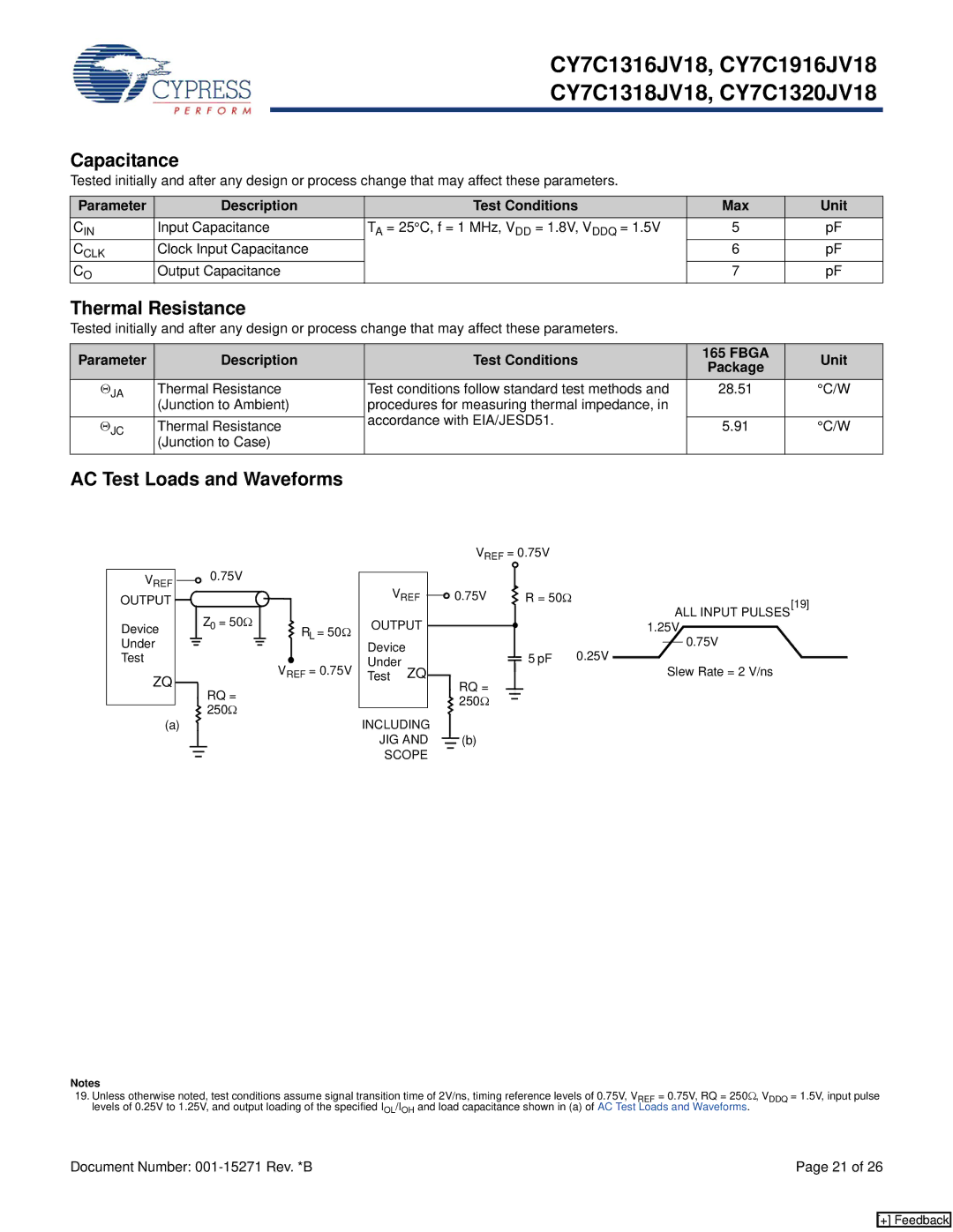
AC Test Loads and Waveforms
VREF = 0.75V
VREF |
|
|
|
|
|
|
| 0.75V |
|
| ||||
|
|
|
|
|
|
|
|
| ||||||
OUTPUT |
|
|
|
|
|
|
|
| Z0 = 50Ω |
|
| |||
|
|
|
|
|
|
|
|
|
| |||||
Device |
|
|
|
|
|
|
|
|
| |||||
Under |
|
|
|
|
|
|
|
|
|
|
|
|
| |
|
|
|
|
|
|
|
|
|
|
|
|
| ||
|
|
|
|
|
|
|
|
|
|
|
|
| ||
Test |
|
|
|
|
|
|
|
|
|
|
|
|
| |
ZQ
RQ =
![]()
![]()
![]() 250Ω
250Ω
(a)
RL = 50Ω
VREF = 0.75V
|
|
|
|
|
|
|
|
|
|
|
|
|
|
|
|
|
|
|
|
|
|
VREF |
|
|
|
|
|
| 0.75V |
|
|
|
|
| R = 50Ω | ||||||||
|
|
|
|
|
|
|
| ||||||||||||||
|
|
|
|
|
|
|
|
| |||||||||||||
OUTPUT |
|
|
|
|
|
|
|
|
|
|
|
|
|
|
|
|
| ALL INPUT PULSES[19] | |||
|
|
|
|
|
|
|
|
|
|
|
|
|
|
|
| ||||||
|
|
|
|
|
|
|
|
|
|
|
|
|
|
| 1.25V | ||||||
|
|
|
|
|
|
|
|
|
|
|
|
|
|
| |||||||
Device |
|
|
|
|
|
|
|
|
|
|
|
|
|
|
|
| 5 pF 0.25V |
|
|
| 0.75V |
|
|
|
|
|
|
|
|
|
|
|
|
|
|
|
|
|
|
| |||
|
|
|
|
|
|
|
|
|
|
|
|
|
|
|
|
|
|
|
| ||
Under | ZQ |
|
|
|
|
|
|
|
|
|
|
|
|
|
|
|
| Slew Rate = 2 V/ns | |||
|
|
|
|
|
|
|
|
|
|
|
|
|
|
| |||||||
|
|
|
|
|
|
|
|
|
|
|
|
|
|
|
| ||||||
Test |
|
|
|
|
|
| RQ = |
|
|
|
|
|
|
|
|
| |||||
|
|
|
|
|
|
|
|
|
|
| |||||||||||
|
|
|
|
|
|
|
|
|
|
|
|
|
|
| |||||||
|
|
|
|
|
|
|
|
|
|
|
|
|
|
|
|
|
|
|
| ||
|
|
|
|
|
|
|
|
|
|
|
|
|
|
|
|
| |||||
|
|
|
|
|
|
|
|
| 250Ω |
|
|
|
|
|
|
|
|
|
| ||
INCLUDING |
|
|
|
|
|
|
|
|
|
|
|
|
|
|
|
| |||||
|
|
|
|
|
|
|
|
|
|
|
|
|
|
|
| ||||||
JIG AND |
|
|
|
|
|
| (b) |
|
|
|
|
|
|
|
|
|
| ||||
|
|
|
|
|
|
|
|
|
|
|
|
|
|
|
| ||||||
|
|
|
|
|
|
|
|
|
|
|
|
|
|
|
| ||||||
SCOPE |
|
|
|
|
|
|
|
|
|
|
|
|
|
|
|
| |||||
Notes
19.Unless otherwise noted, test conditions assume signal transition time of 2V/ns, timing reference levels of 0.75V, VREF = 0.75V, RQ = 250Ω, VDDQ = 1.5V, input pulse levels of 0.25V to 1.25V, and output loading of the specified IOL/IOH and load capacitance shown in (a) of AC Test Loads and Waveforms.
Document Number: | Page 21 of 26 |
[+] Feedback