CY7C1316JV18, CY7C1916JV18 CY7C1318JV18, CY7C1320JV18
driver impedance. The value of RQ must be 5x the value of the intended line impedance driven by the SRAM. The allowable range of RQ to guarantee impedance matching with a tolerance of ±15% is between 175Ω and 350Ω, with VDDQ = 1.5V. The output impedance is adjusted every 1024 cycles at power up to account for drifts in supply voltage and temperature.
Echo Clocks
Echo clocks are provided on the
DLL
These chips use a Delay Lock Loop (DLL) that is designed to function between 120 MHz and the specified maximum clock frequency. During power up, when the DOFF is tied HIGH, the DLL is locked after 1024 cycles of stable clock. The DLL can also be reset by slowing or stopping the input clocks K and K for a minimum of 30 ns. However, it is not necessary for the to specif- ically reset the DLL to lock it to the desired frequency. The DLL automatically locks 1024 clock cycles after a stable clock is presented. The DLL may be disabled by applying ground to the DOFF pin. When the DLL is turned off, the device behaves in
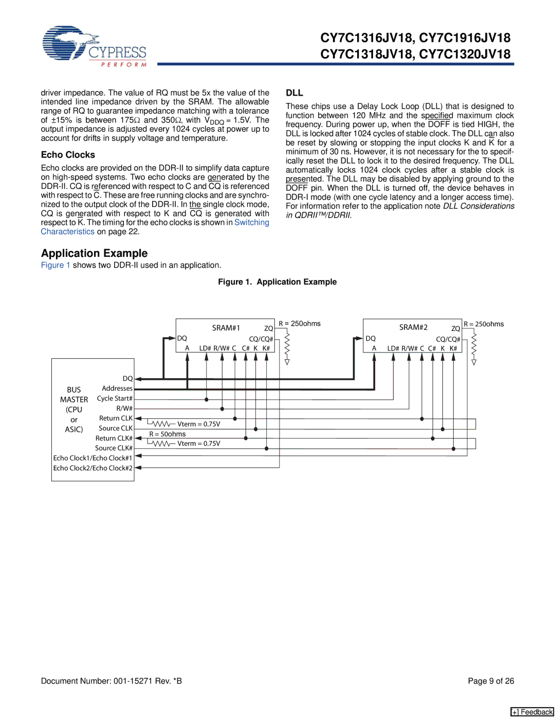
SRAM#1 ZQ
![]() DQCQ/CQ#
DQCQ/CQ#
A LD# R/W# C C# K K#
| DQ |
| |
BUS | Addresses |
| |
MASTER | Cycle Start# |
| |
(CPU | R/W# |
| |
or | Return CLK | Vterm = 0.75V | |
ASIC) | Source CLK | ||
R = 50ohms | |||
| Return CLK# | ||
| Vterm = 0.75V | ||
| Source CLK# | ||
|
| ||
Echo Clock1/Echo Clock#1 |
| ||
Echo Clock2/Echo Clock#2 |
| ||
R = 250ohms | SRAM#2 |
| ZQ | ||||
|
|
| |||||
|
| DQ | CQ/CQ# | ||||
|
| ||||||
|
| A LD# R/W# C C# | K K# | ||||
|
|
|
|
|
|
|
|
|
|
|
|
|
|
|
|
|
|
|
|
|
|
|
|
|
|
|
|
|
|
|
|
|
|
|
|
|
|
|
|
|
|
|
|
|
|
|
|
R = 250ohms
Document Number: | Page 9 of 26 |
[+] Feedback