CY7C1316JV18, CY7C1916JV18
CY7C1318JV18, CY7C1320JV18
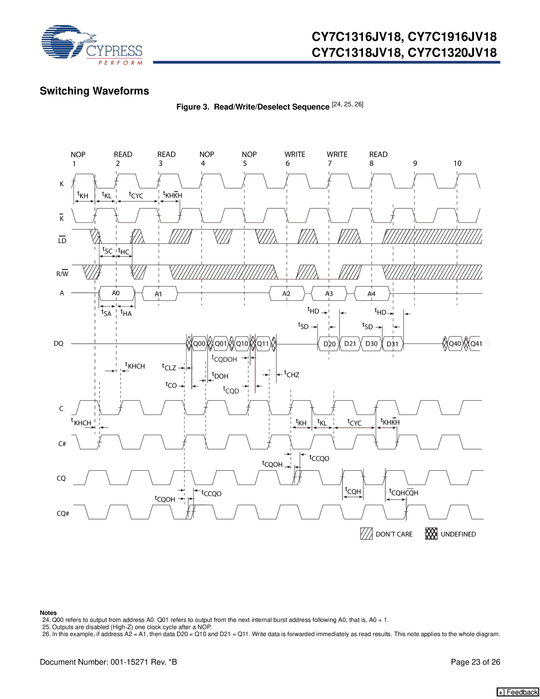
Switching Waveforms
Figure 3. Read/Write/Deselect Sequence [24, 25, 26]
NOP |
| READ | READ |
1 |
| 2 | 3 |
K |
|
|
|
tKH | tKL | tCYC | tKHKH |
K |
|
|
|
LD | tSC |
|
|
| tHC |
| |
R/W |
|
|
|
NOP | NOP | WRITE | WRITE | READ |
|
|
| ||
4 | 5 | 6 | 7 | 8 | 9 | 10 | |||
|
|
|
|
|
|
|
|
|
|
|
|
|
|
|
|
|
|
|
|
A | A0 | A1 |
tSA |
| tHA |
DQ
tKHCH tCLZ ![]() tCO
tCO ![]()
C
A2 | A3 |
tHD
tSD
Q00 Q01 Q10 | Q11 |
tCQDOH |
|
tDOH | tCHZ |
tCQD |
|
A4
tHD
tSD
D21 | D30 | D31 |
![]()
![]() Q41
Q41 ![]()
t KHCH
C#
tKH tKL |
| tCYC | tKHKH |
|
| ||||
|
|
|
|
|
|
|
|
|
|
|
|
|
|
|
|
|
|
|
|
CQ
tCQOH
tCCQO
tCQOH ![]()
CQ#
tCCQO | tCQH |
| tCQHCQH | ||||
|
|
|
|
|
|
|
|
|
|
|
|
|
|
|
|
DON’T CARE
UNDEFINED
Notes
24.Q00 refers to output from address A0. Q01 refers to output from the next internal burst address following A0, that is, A0 + 1.
25.Outputs are disabled
26.In this example, if address A2 = A1, then data D20 = Q10 and D21 = Q11. Write data is forwarded immediately as read results. This note applies to the whole diagram.
Document Number: | Page 23 of 26 |
[+] Feedback