Functional Description
Features
Configurations
CY7C1316JV18, CY7C1916JV18 CY7C1318JV18, CY7C1320JV18
+ Feedback
Logic Block Diagram CY7C1316JV18
Logic Block Diagram CY7C1916JV18
CY7C1316JV18, CY7C1916JV18 CY7C1318JV18, CY7C1320JV18
+ Feedback
Logic Block Diagram CY7C1318JV18
Logic Block Diagram CY7C1320JV18
CY7C1316JV18, CY7C1916JV18 CY7C1318JV18, CY7C1320JV18
165-Ball FBGA 13 x 15 x 1.4 mm Pinout
Pin Configuration
CY7C1316JV18, CY7C1916JV18 CY7C1318JV18, CY7C1320JV18
Pin Configuration
165-Ball FBGA 13 x 15 x 1.4 mm Pinout
CY7C1318JV18, CY7C1320JV18
CY7C1316JV18, CY7C1916JV18
Pin Definitions
Pin Definitions continued
CY7C1318JV18, CY7C1320JV18
CY7C1316JV18, CY7C1916JV18
Write Operations
Single Clock Mode
Functional Overview
Read Operations
Echo Clocks
Application Example
CY7C1316JV18, CY7C1916JV18 CY7C1318JV18, CY7C1320JV18
Write Cycle Descriptions
Truth Table
Burst Address Table
Write Cycle Descriptions
CY7C1316JV18, CY7C1916JV18 CY7C1318JV18, CY7C1320JV18
Write Cycle Descriptions
Performing a TAP Reset
Disabling the JTAG Feature
Test Access Port-Test Clock
Test Mode Select TMS
BYPASS
IDCODE
SAMPLE Z
SAMPLE/PRELOAD
CY7C1316JV18, CY7C1916JV18 CY7C1318JV18, CY7C1320JV18
TAP Controller State Diagram
Page 14 of
TAP Electrical Characteristics
TAP Controller Block Diagram
CY7C1316JV18, CY7C1916JV18 CY7C1318JV18, CY7C1320JV18
TAP Timing and Test Conditions
TAP AC Switching Characteristics
CY7C1316JV18, CY7C1916JV18 CY7C1318JV18, CY7C1320JV18
Identification Register Definitions
Scan Register Sizes
Instruction Codes
CY7C1316JV18, CY7C1916JV18 CY7C1318JV18, CY7C1320JV18
Boundary Scan Order
DLL Constraints
Power Up Sequence in DDR-II SRAM
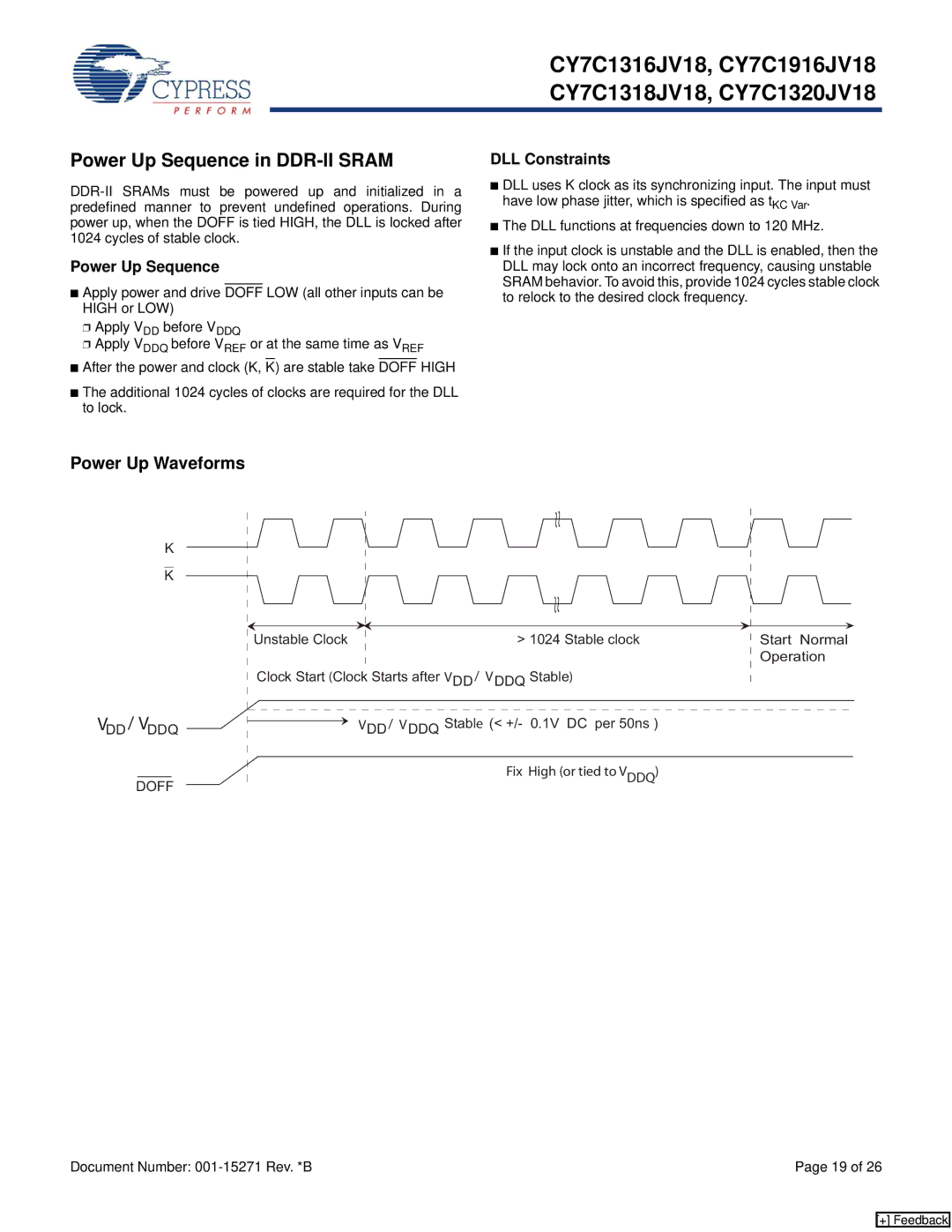
Power Up Waveforms
Power Up Sequence
Maximum Ratings
Electrical Characteristics
DC Electrical Characteristics
AC Electrical Characteristics
CY7C1316JV18, CY7C1916JV18 CY7C1318JV18, CY7C1320JV18
Capacitance
Thermal Resistance
AC Test Loads and Waveforms
Parameter
Switching Characteristics
CY7C1316JV18, CY7C1916JV18
CY7C1318JV18, CY7C1320JV18
tCQD
Switching Waveforms
CY7C1316JV18, CY7C1916JV18 CY7C1318JV18, CY7C1320JV18
tCQDOH
CY7C1316JV18, CY7C1916JV18 CY7C1318JV18, CY7C1320JV18
Ordering Information
+ Feedback
Package Diagram
CY7C1316JV18, CY7C1916JV18 CY7C1318JV18, CY7C1320JV18
Figure 4. 165-ball FBGA 13 x 15 x 1.40 mm
Burst Architecture Document Number
Document History Page
ISSUE
CY7C1316JV18, CY7C1916JV18 CY7C1318JV18, CY7C1320JV18