CY7C1316JV18, CY7C1916JV18
CY7C1318JV18, CY7C1320JV18
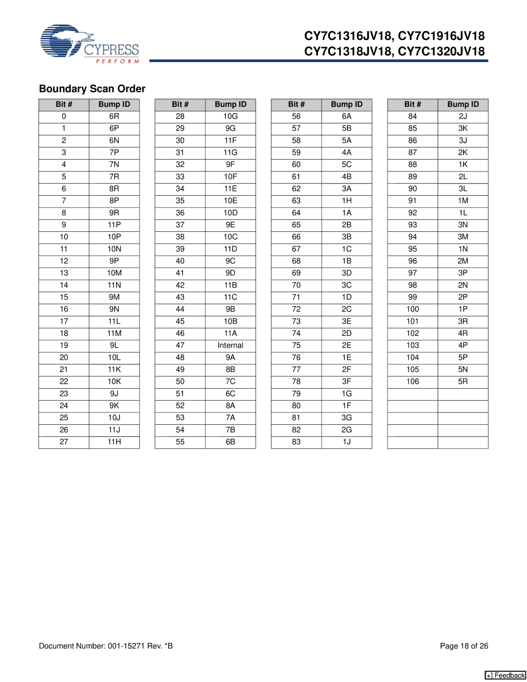
Boundary Scan Order
Bit # | Bump ID |
| Bit # | Bump ID |
| Bit # | Bump ID |
| Bit # | Bump ID |
0 | 6R |
| 28 | 10G |
| 56 | 6A |
| 84 | 2J |
|
|
|
|
|
|
|
|
|
|
|
1 | 6P |
| 29 | 9G |
| 57 | 5B |
| 85 | 3K |
|
|
|
|
|
|
|
|
|
|
|
2 | 6N |
| 30 | 11F |
| 58 | 5A |
| 86 | 3J |
|
|
|
|
|
|
|
|
|
|
|
3 | 7P |
| 31 | 11G |
| 59 | 4A |
| 87 | 2K |
|
|
|
|
|
|
|
|
|
|
|
4 | 7N |
| 32 | 9F |
| 60 | 5C |
| 88 | 1K |
|
|
|
|
|
|
|
|
|
|
|
5 | 7R |
| 33 | 10F |
| 61 | 4B |
| 89 | 2L |
|
|
|
|
|
|
|
|
|
|
|
6 | 8R |
| 34 | 11E |
| 62 | 3A |
| 90 | 3L |
|
|
|
|
|
|
|
|
|
|
|
7 | 8P |
| 35 | 10E |
| 63 | 1H |
| 91 | 1M |
|
|
|
|
|
|
|
|
|
|
|
8 | 9R |
| 36 | 10D |
| 64 | 1A |
| 92 | 1L |
|
|
|
|
|
|
|
|
|
|
|
9 | 11P |
| 37 | 9E |
| 65 | 2B |
| 93 | 3N |
|
|
|
|
|
|
|
|
|
|
|
10 | 10P |
| 38 | 10C |
| 66 | 3B |
| 94 | 3M |
|
|
|
|
|
|
|
|
|
|
|
11 | 10N |
| 39 | 11D |
| 67 | 1C |
| 95 | 1N |
|
|
|
|
|
|
|
|
|
|
|
12 | 9P |
| 40 | 9C |
| 68 | 1B |
| 96 | 2M |
|
|
|
|
|
|
|
|
|
|
|
13 | 10M |
| 41 | 9D |
| 69 | 3D |
| 97 | 3P |
|
|
|
|
|
|
|
|
|
|
|
14 | 11N |
| 42 | 11B |
| 70 | 3C |
| 98 | 2N |
|
|
|
|
|
|
|
|
|
|
|
15 | 9M |
| 43 | 11C |
| 71 | 1D |
| 99 | 2P |
|
|
|
|
|
|
|
|
|
|
|
16 | 9N |
| 44 | 9B |
| 72 | 2C |
| 100 | 1P |
|
|
|
|
|
|
|
|
|
|
|
17 | 11L |
| 45 | 10B |
| 73 | 3E |
| 101 | 3R |
|
|
|
|
|
|
|
|
|
|
|
18 | 11M |
| 46 | 11A |
| 74 | 2D |
| 102 | 4R |
|
|
|
|
|
|
|
|
|
|
|
19 | 9L |
| 47 | Internal |
| 75 | 2E |
| 103 | 4P |
|
|
|
|
|
|
|
|
|
|
|
20 | 10L |
| 48 | 9A |
| 76 | 1E |
| 104 | 5P |
|
|
|
|
|
|
|
|
|
|
|
21 | 11K |
| 49 | 8B |
| 77 | 2F |
| 105 | 5N |
|
|
|
|
|
|
|
|
|
|
|
22 | 10K |
| 50 | 7C |
| 78 | 3F |
| 106 | 5R |
|
|
|
|
|
|
|
|
|
|
|
23 | 9J |
| 51 | 6C |
| 79 | 1G |
|
|
|
|
|
|
|
|
|
|
|
|
|
|
24 | 9K |
| 52 | 8A |
| 80 | 1F |
|
|
|
|
|
|
|
|
|
|
|
|
|
|
25 | 10J |
| 53 | 7A |
| 81 | 3G |
|
|
|
|
|
|
|
|
|
|
|
|
|
|
26 | 11J |
| 54 | 7B |
| 82 | 2G |
|
|
|
|
|
|
|
|
|
|
|
|
|
|
27 | 11H |
| 55 | 6B |
| 83 | 1J |
|
|
|
|
|
|
|
|
|
|
|
|
|
|
Document Number: | Page 18 of 26 |
[+] Feedback