CY25818/19

Table 5. Timing Electrical Characteristics Vdd = 3.3V ±10%, TA = 0°C to +70°C and CL = 15 pF (unless otherwise noted)

Parameter

Description

Conditions

Min.

Typ.

Max.

Unit

ICLKFR1

Input Frequency Range

CY25818

8

16

MHz


ICLKFR2

Input Frequency Range

CY25819

16

32

MHz


trise1

Clock Rise Time

SSCLK and REFCLK, 0.4V to 2.4V

2.0

3.0

4.0

ns


tfall1

Clock Fall Time

SSCLK and REFCLK, 0.4V to 2.4V

2.0

3.0

4.0

ns


CDCin

Input Clock Duty Cycle

XIN

20

50

80

%

CDCout

Output Clock Duty Cycle

SSCLK and REFCLK @ 1.5V

45

50

55

%


CCJss

Cycle-to-Cycle Jitter

SSCLK; FIN = FOUT = 8–32 MHz


250

350

ps

CCJref

Cycle-to-Cycle Jitter

REFCLK; FIN = FOUT = 8–32 MHz


275

375

ps

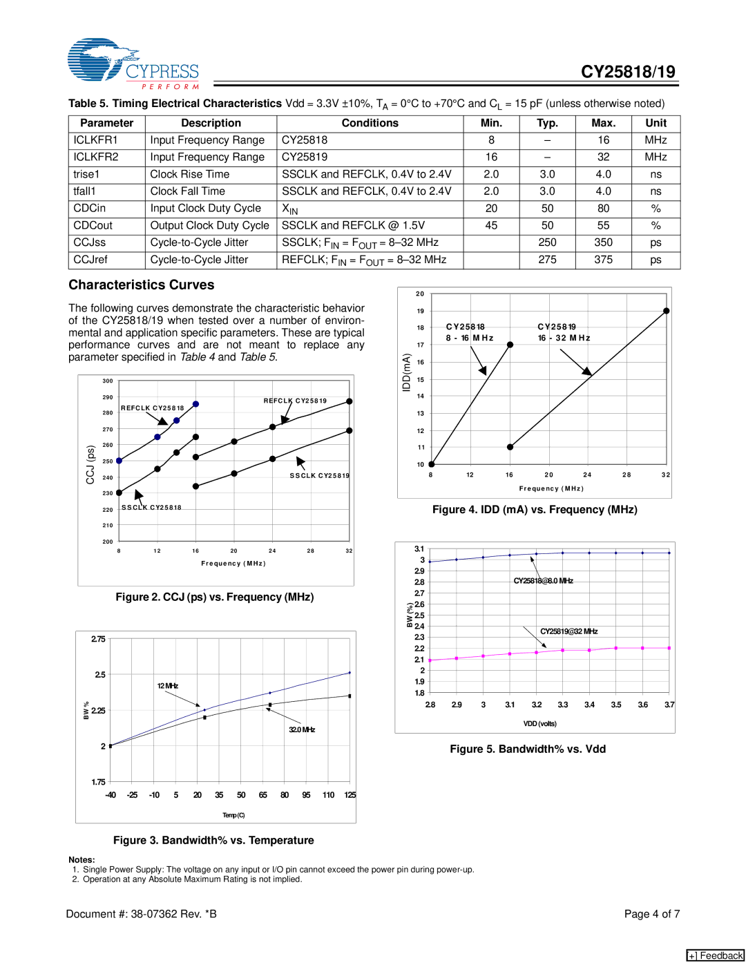
Characteristics Curves

The following curves demonstrate the characteristic behavior of the CY25818/19 when tested over a number of environ- mental and application specific parameters. These are typical performance curves and are not meant to replace any parameter specified in Table 4 and Table 5.


300


290


REFCLK CY2 5 8 19


REFCLK CY2 5 8 18


280


270


(ps)

260


250


CCJ


240


S S CLK CY2 5 8 19


230


220

S S CLK CY2 5 8 18


210


200


8

12

16

20

24

28

32


Fr e que nc y ( M Hz )


Figure 2. CCJ (ps) vs. Frequency (MHz)


2.75


2.5


12MHz


%

2.25


BW


32.0MHz


2


1.75


-40

-25

-10

5

20

35

50

65

80

95

110

125


Temp(C)


2 0


19


18

C Y25818


C Y25819


17

8 - 16 M H z


16 - 32 M H z


IDD(mA)

16


15


14


13


12


11


10


8

12

16

2 0

2 4

2 8

3 2


Fr e que nc y ( M Hz )


Figure 4. IDD (mA) vs. Frequency (MHz)


3.1


3


2.9


CY25818@8.0 MHz


2.8


2.7


(%)

2.6


2.5


BW


2.4


CY25819@32 MHz


2.3


2.2


2.1


2


1.9


1.8


2.8

2.9

3

3.1

3.2

3.3

3.4

3.5

3.6

3.7

VDD (volts)

Figure 5. Bandwidth% vs. Vdd

Figure 3. Bandwidth% vs. Temperature

Notes:

1.Single Power Supply: The voltage on any input or I/O pin cannot exceed the power pin during power-up.

2.Operation at any Absolute Maximum Rating is not implied.

Document #: 38-07362 Rev. *B

Page 4 of 7

[+] Feedback

Page 4
Image 4
Cypress CY25819, CY25818 manual Characteristics Curves, ICLKFR1, ICLKFR2

CY25819, CY25818 specifications

Cypress Semiconductor, a renowned player in the embedded solutions market, has introduced two advanced clock generators: the CY25819 and CY25818. These devices stand out in the realm of high-performance clock management solutions, offering a variety of features that make them ideal for various applications such as telecommunications, consumer electronics, and computing systems.

The CY25819 and CY25818 utilize cutting-edge technology to provide users with exceptional flexibility and reliability. Both devices are designed to generate multiple clock outputs from a single reference clock input, which ultimately reduces component count and simplifies circuit design. This is especially valuable in modern electronic designs that prioritize space efficiency and power reduction.

One of the key features of the CY25819 is its ability to produce up to nine output clocks, while the CY25818 generates up to six. This capability allows designers to meet the diverse timing requirements of complex systems seamlessly. Additionally, both models support a wide range of output frequencies, which can be easily configured through I2C communication. This programmability ensures that designers can adapt the device to their specific needs, enhancing its versatility for different applications.

In terms of performance characteristics, both the CY25819 and CY25818 exhibit low phase noise and jitter, critical metrics for applications where timing precision is paramount. The low jitter performance is particularly important in high-speed data transfers and communication interfaces, as it helps maintain signal integrity and minimize errors.

Another notable feature includes power management capabilities. The CY25819 and CY25818 provide multiple power-saving modes, such as a low power sleep mode, which significantly reduces power consumption when the system is idle. This energy-efficient design is aligned with the growing demand for sustainable electronic solutions and extends battery life in portable applications.

Furthermore, these devices are built with robust engineering to ensure high reliability under various operating conditions. They offer a wide temperature range, making them suitable for industrial applications.

In summary, the Cypress CY25819 and CY25818 clock generators are exceptional solutions tailored for complex timing needs in a diverse array of industries. With their high output capabilities, superior performance, energy-efficient features, and reliability, they represent the forefront of clock management technology, enabling engineers to innovate and optimize their designs effectively.