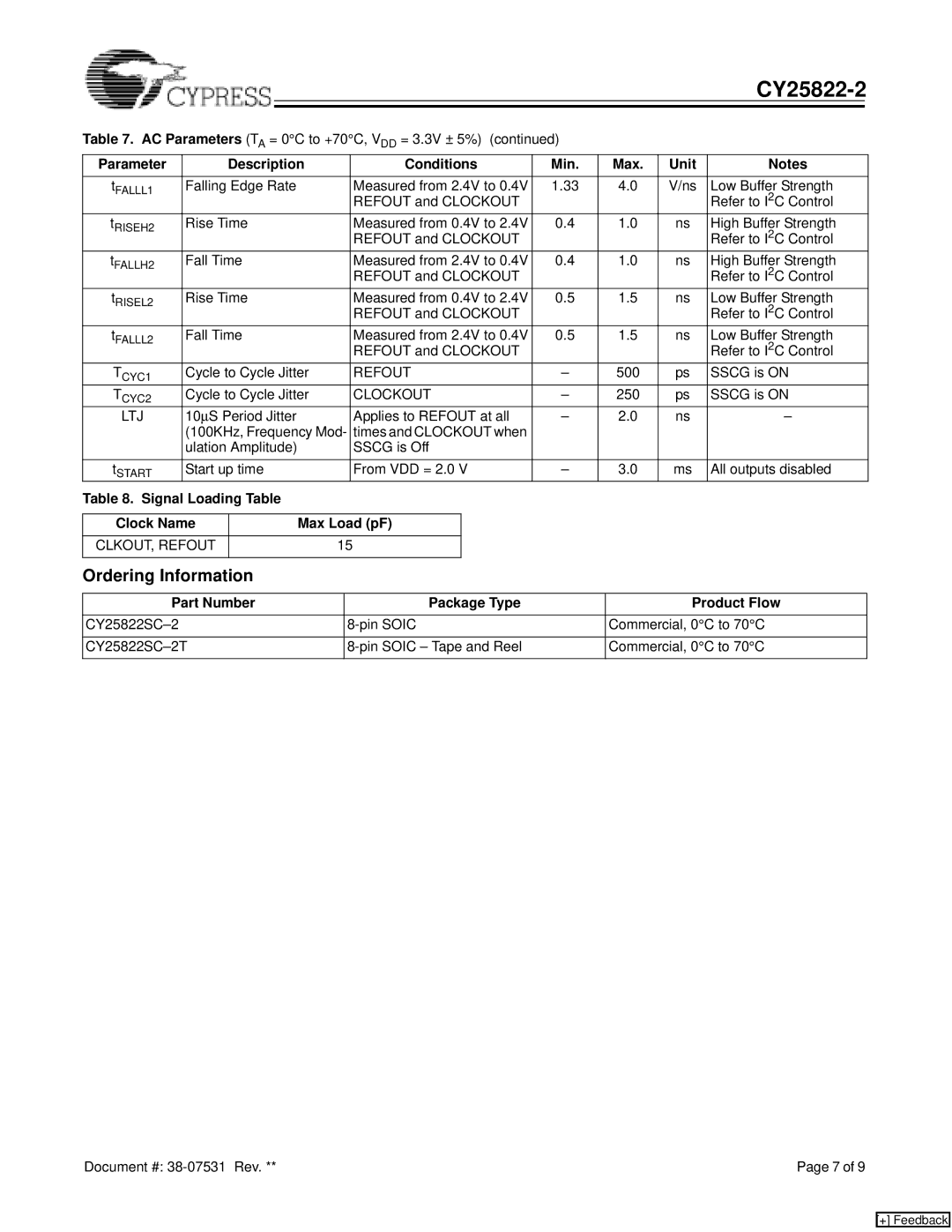
CY25822-2 specifications
The Cypress CY25822-2 is a highly versatile clock generator and clock distribution device designed for use in high-performance applications. As part of Cypress's extensive portfolio of timing solutions, the CY25822-2 takes center stage in delivering precise clock signals for system synchronization and performance enhancement.One of the standout features of the CY25822-2 is its ability to generate multiple output clocks from a single input source. This functionality is particularly beneficial in applications where multiple components or subsystems require synchronized clock signals, allowing designers to simplify their designs and reduce component count.
The CY25822-2 supports a wide input frequency range, accommodating various system clock sources while maintaining low jitter performance. This characteristic is critical in high-speed digital applications, where timing precision is paramount. With its ability to minimize phase noise and jitter, the CY25822-2 ensures reliable data transmission and system stability.
Another notable aspect of the CY25822-2 is its programmable features. The device can be configured through a simple interface, allowing designers to customize the output frequencies and clock characteristics according to their specific application needs. This programmability enhances flexibility, enabling the CY25822-2 to be used in diverse environments, from consumer electronics to automotive systems.
The CY25822-2 utilizes advanced phase-locked loop (PLL) technology to achieve high-performance clock generation. The PLL feature allows it to multiply input frequencies and generate higher frequency outputs while maintaining excellent signal integrity. This capability is crucial for modern high-speed data applications, including networking, telecommunications, and high-definition video processing.
In terms of power efficiency, the CY25822-2 is designed to operate with low power consumption, making it suitable for battery-operated devices and energy-sensitive applications. The reduced power footprint contributes to prolonged battery life and better overall system performance.
Moreover, the CY25822-2 package options cater to various design requirements, offering flexibility for integration into a range of PCB layouts. Its small footprint suits compact devices, while its robust operation ensures reliability across different environmental conditions.
In conclusion, the Cypress CY25822-2 stands out as a reliable and advanced clock generator solution, integrating essential features such as multiple outputs, low jitter performance, programmability, and power efficiency. Its adoption across various high-performance applications underscores its importance in the modern electronics landscape.

