|
|
|
| ||
7. Pin Description |
|
|
| ||
Tx/Rx | Pin No. | I/O | Pin Name | Description | |
| 1 |
| VeeR | Receiver Ground | |
| 2 |
| VccR | +3.3V Receiver Power Supply | |
Rx | 3 | O | SD | Normal Optical Input indicated by logic “High”, and No Optical | |
| Input indicated by logic “Low”. (LVTTL) | ||||
|
|
|
| ||
| 4 | O | RD(n) | Inverted Receiver Data Output | |
| 5 | O | RD(p) | ||
| 6 |
| VccT | +3.3V Transmitter Power Supply | |
Tx | 7 |
| VeeT | Transmitter Ground | |
8 | I | BiasCNT | Positive pulse which control the ONU burst mode operation | ||
| 9 | I | TD(p) | ||
| 10 | I | TD(n) | Inverted Transmitter Data Input | |
|
|
| MS | Mounting studs/ connect this pin to Chassis ground | |
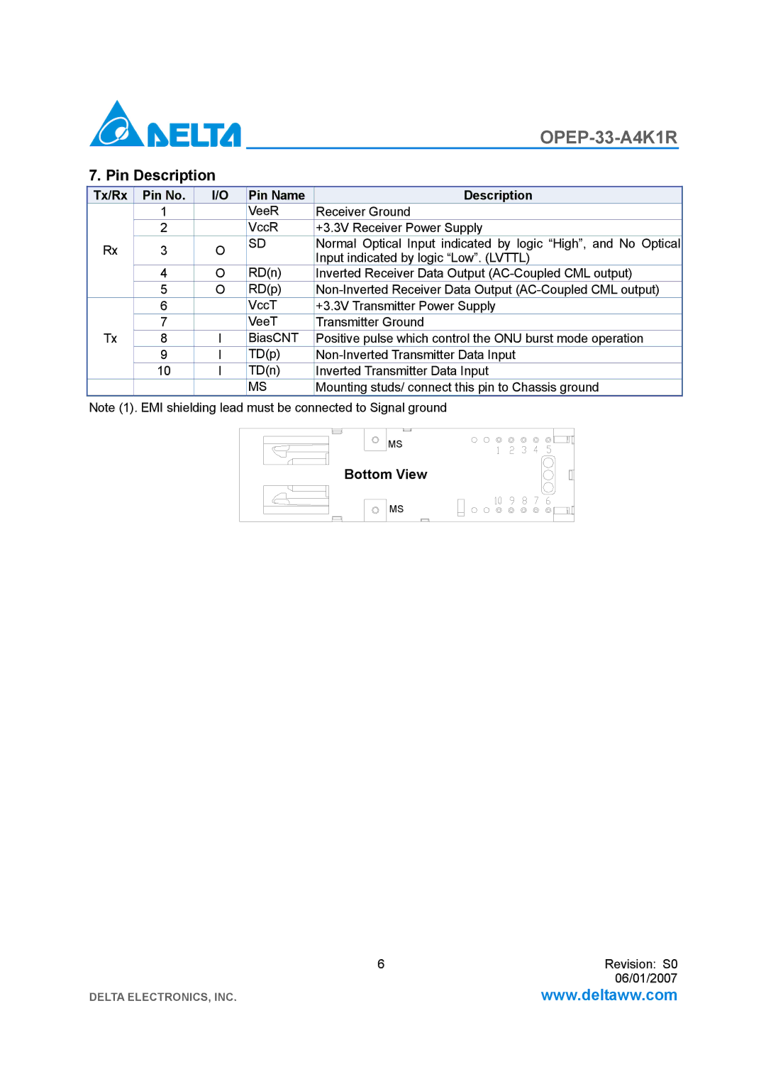
Note (1). EMI shielding lead must be connected to Signal ground
MS
Bottom View
MS
6 | Revision: S0 |
| 06/01/2007 |
DELTA ELECTRONICS, INC. | www.deltaww.com |