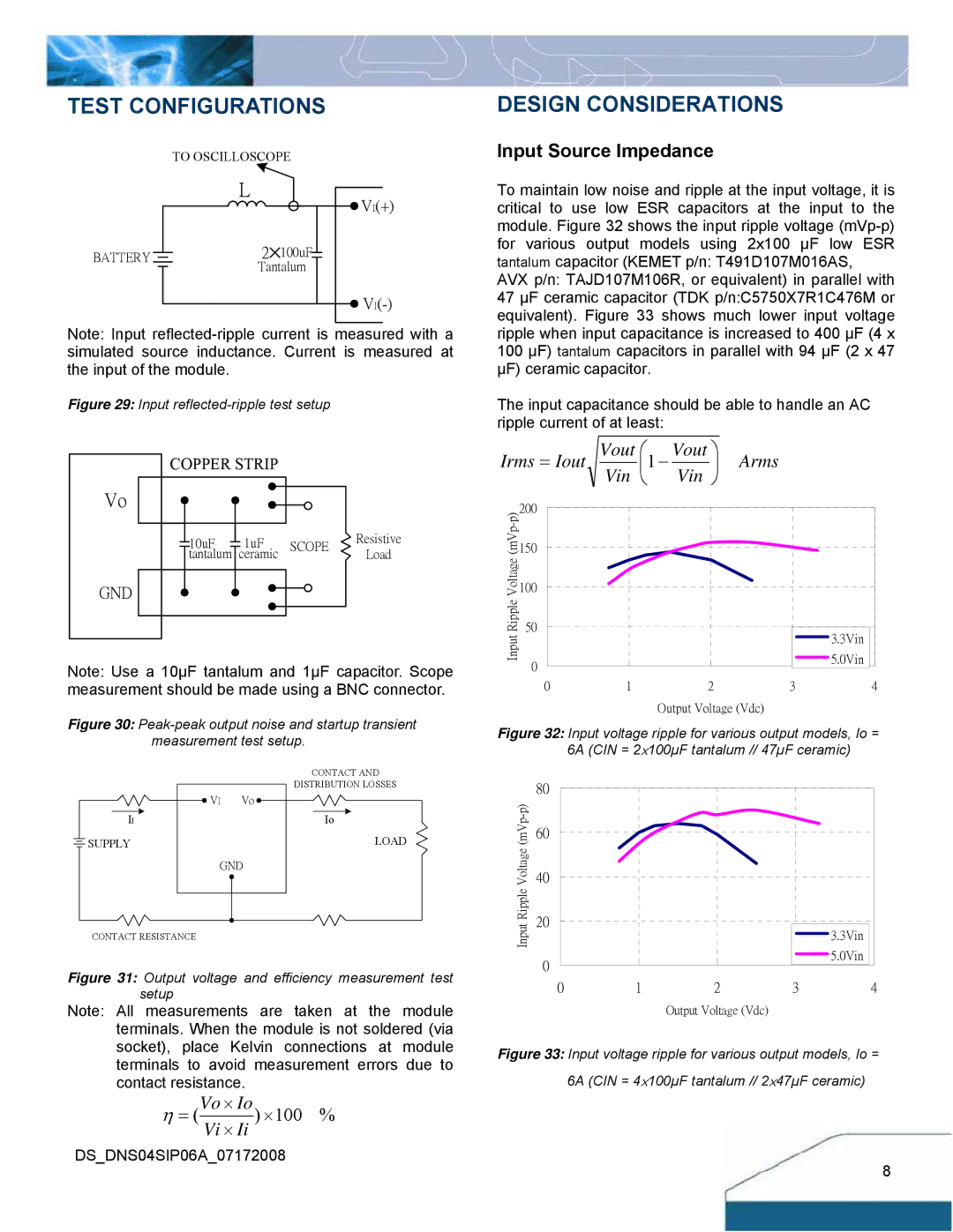
TEST CONFIGURATIONS
| TO OSCILLOSCOPE | |
| L | VI(+) |
|
| |
BATTERY | 2 | 100uF |
| Tantalum | |
|
| |
Note: Input
Figure 29: Input reflected-ripple test setup
COPPER STRIP
Vo
| 10uF |
| 1uF | SCOPE | Resistive |
|
| ||||
tantalum | ceramic | Load | |||
GND
Note: Use a 10μF tantalum and 1μF capacitor. Scope measurement should be made using a BNC connector.
Figure 30: Peak-peak output noise and startup transient measurement test setup.
|
|
|
|
|
| CONTACT AND | ||
|
|
|
|
|
| DISTRIBUTION LOSSES | ||
|
|
| VI | Vo |
| |||
|
|
|
|
|
|
| ||
|
|
|
|
|
|
| ||
|
|
|
|
|
|
|
| |
| II |
|
|
|
|
| Io |
|
SUPPLY |
|
|
|
|
| LOAD | ||
|
|
| GND |
|
|
| ||
|
|
|
|
|
|
|
|
|
CONTACT RESISTANCE
Figure 31: Output voltage and efficiency measurement test setup
Note: All measurements are taken at the module terminals. When the module is not soldered (via socket), place Kelvin connections at module terminals to avoid measurement errors due to contact resistance.
η = (Vo ⋅ Io) ⋅100 %
Vi ⋅ Ii
DS_DNS04SIP06A_07172008
DESIGN CONSIDERATIONS
Input Source Impedance
To maintain low noise and ripple at the input voltage, it is critical to use low ESR capacitors at the input to the module. Figure 32 shows the input ripple voltage
The input capacitance should be able to handle an AC ripple current of at least:
Irms = Iout | Vout ⎛ | − | Vout ⎞ | Arms |
| |||
Vin | ⎜1 | Vin | ⎟ |
| ||||
|
| ⎝ |
| ⎠ |
|
| ||
200 |
|
|
|
|
|
|
| |
150 |
|
|
|
|
|
|
| |
Ripple Voltage | 100 |
|
|
|
|
|
|
|
50 |
|
|
|
|
|
| 3.3Vin | |
Input |
|
|
|
|
|
|
| |
0 |
|
|
|
|
|
| 5.0Vin | |
|
|
|
|
|
|
| ||
|
|
|
|
|
|
|
| |
| 0 | 1 |
|
|
| 2 | 3 | 4 |
Output Voltage (Vdc)
Figure 32: Input voltage ripple for various output models, Io = 6A (CIN = 2×100µF tantalum // 47µF ceramic)
| 80 |
|
|
|
|
40 |
|
|
|
| |
Voltage(mVp |
|
|
|
| |
| 60 |
|
|
|
|
Ripple | 20 |
|
|
|
|
Input |
|
|
| 3.3Vin | |
|
|
|
| ||
|
|
|
|
| |
| 0 |
|
|
| 5.0Vin |
|
|
|
|
| |
| 0 | 1 | 2 | 3 | 4 |
Output Voltage (Vdc)
Figure 33: Input voltage ripple for various output models, Io =
6A (CIN = 4×100µF tantalum // 2×47µF ceramic)
8