F i n i s a r |
Diagram of Host Board Connector Block Pin Numbers and Names
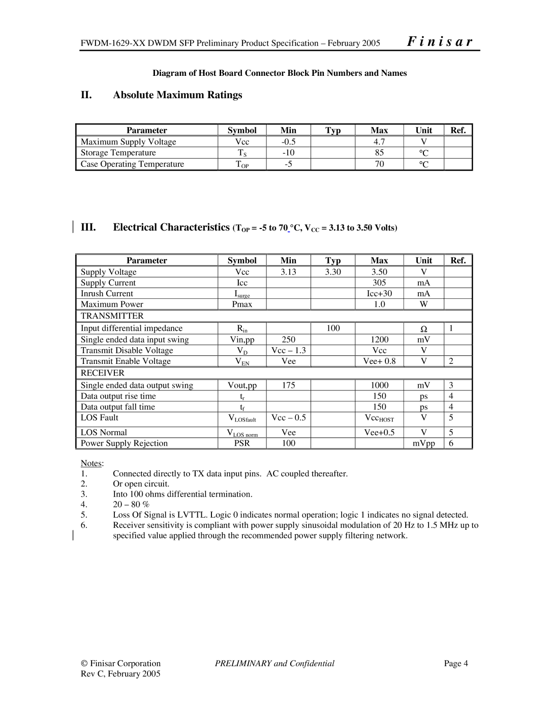
II.Absolute Maximum Ratings
Parameter | Symbol | Min | Typ | Max | Unit | Ref. |
Maximum Supply Voltage | Vcc |
| 4.7 | V |
| |
Storage Temperature | TS |
| 85 | °C |
| |
Case Operating Temperature | TOP |
| 70 | °C |
|
III.Electrical Characteristics (TOP =
Parameter | Symbol | Min | Typ | Max | Unit | Ref. |
Supply Voltage | Vcc | 3.13 | 3.30 | 3.50 | V |
|
Supply Current | Icc |
|
| 305 | mA |
|
Inrush Current | Isurge |
|
| Icc+30 | mA |
|
Maximum Power | Pmax |
|
| 1.0 | W |
|
TRANSMITTER |
|
|
|
|
|
|
Input differential impedance | Rin |
| 100 |
| Ω | 1 |
Single ended data input swing | Vin,pp | 250 |
| 1200 | mV |
|
Transmit Disable Voltage | VD | Vcc – 1.3 |
| Vcc | V |
|
Transmit Enable Voltage | VEN | Vee |
| Vee+ 0.8 | V | 2 |
RECEIVER |
|
|
|
|
|
|
Single ended data output swing | Vout,pp | 175 |
| 1000 | mV | 3 |
Data output rise time | tr |
|
| 150 | ps | 4 |
Data output fall time | tf |
|
| 150 | ps | 4 |
LOS Fault | VLOSfault | Vcc – 0.5 |
| VccHOST | V | 5 |
LOS Normal | VLOS norm | Vee |
| Vee+0.5 | V | 5 |
Power Supply Rejection | PSR | 100 |
|
| mVpp | 6 |
Notes:
1.Connected directly to TX data input pins. AC coupled thereafter.
2.Or open circuit.
3.Into 100 ohms differential termination.
4.20 – 80 %
5.Loss Of Signal is LVTTL. Logic 0 indicates normal operation; logic 1 indicates no signal detected.
6.Receiver sensitivity is compliant with power supply sinusoidal modulation of 20 Hz to 1.5 MHz up to specified value applied through the recommended power supply filtering network.
© Finisar Corporation | PRELIMINARY and Confidential | Page 4 |
Rev C, February 2005 |
|
|
