130nm node CMOS Process (CS90A)
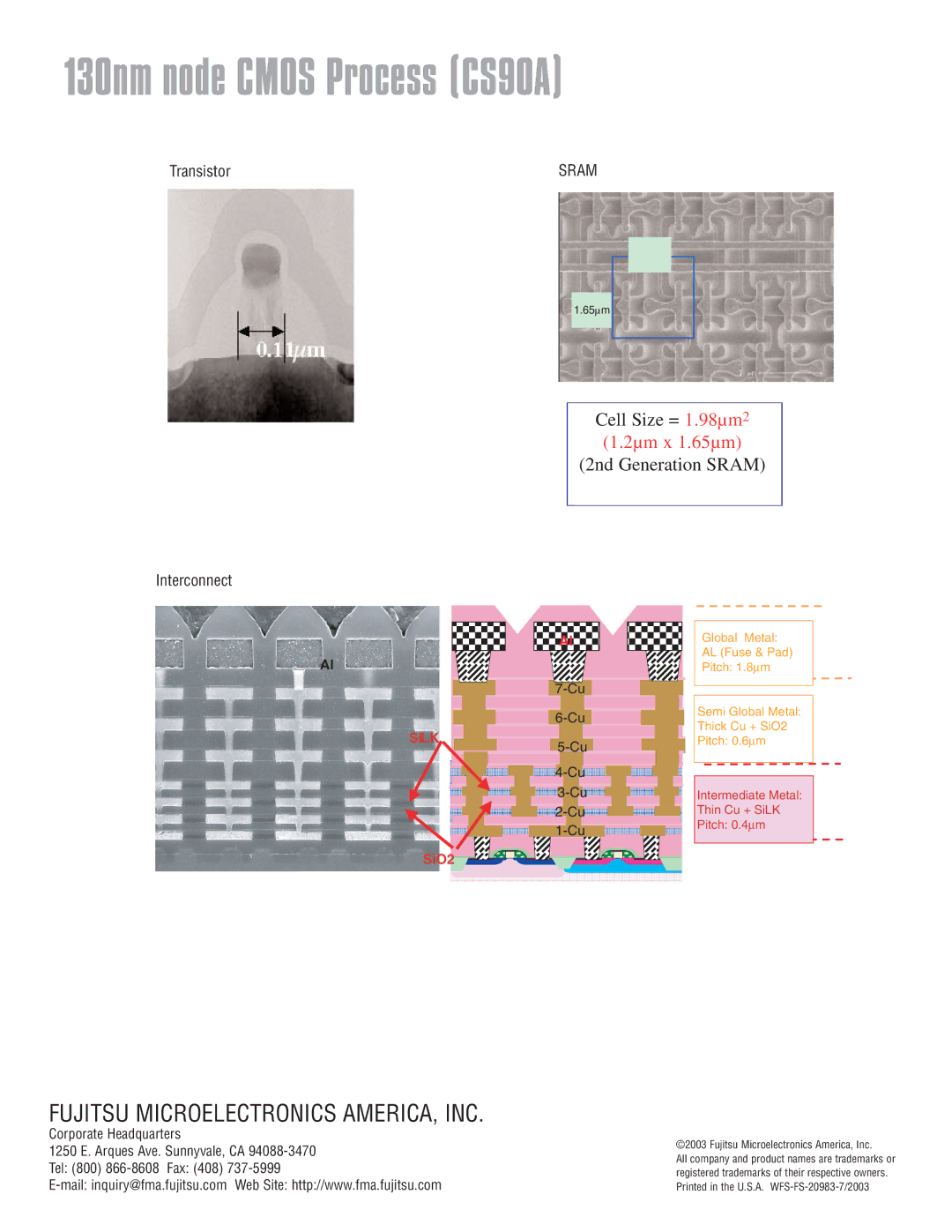
Transistor | SRAM |
1.65µm
Cell Size = 1.98µm2
(1.2µm x 1.65µm)
(2nd Generation SRAM)
Interconnect
Al
Al
SiLK
![]()
![]()
![]() 3-Cu
3-Cu
SiO2 


Global Metal:
AL (Fuse & Pad)
Pitch: 1.8∝m
Semi Global Metal:
Thick Cu + SiO2
Pitch: 0.6∝m
Intermediate Metal:
Thin Cu + SiLK
Pitch: 0.4∝m
FUJITSU MICROELECTRONICS AMERICA, INC.
Corporate Headquarters
1250 E. Arques Ave. Sunnyvale, CA
©2003 Fujitsu Microelectronics America, Inc.
All company and product names are trademarks or registered trademarks of their respective owners. Printed in the U.S.A.