Upgrading main memory
Upgrading main memory
Technical data
Technology: | DDR 266, DDR 333 or DDR 400 unbuffered DIMM modules |
| |
Size: | 128 Mbytes up to 4 Gbyte DDR 266 SDRAM |
| 128 Mbytes up to Gbyte DDR 333 SDRAM |
| 128 Mbytes up to Gbyte DDR 400 SDRAM |
Granularity: | 128, 256, 512 or 1024 Mbyte for one socket |
A current list of the memory modules recommended for this mainboard is available on the Internet at:
At least one memory module must be installed. Memory modules with different memory capacities can be combined.
You may only use unbuffered 2,5 V memory modules. Buffered memory modules are not ! supported.
specification.
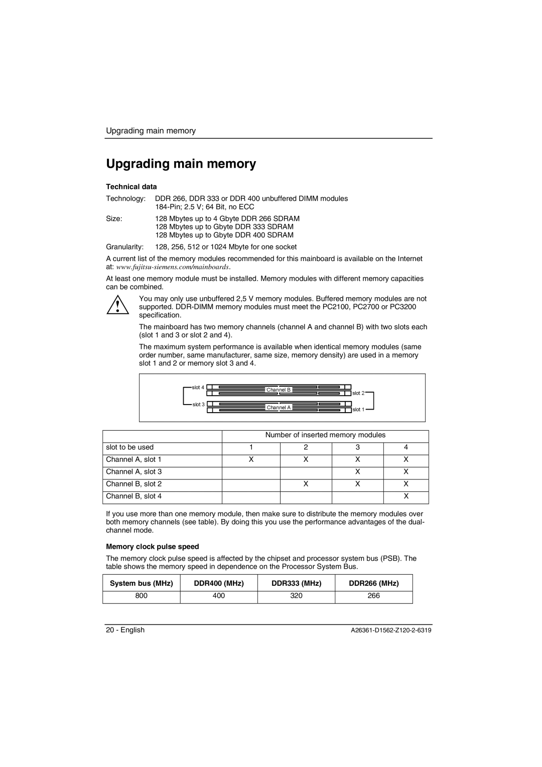
The mainboard has two memory channels (channel A and channel B) with two slots each (slot 1 and 3 or slot 2 and 4).
The maximum system performance is available when identical memory modules (same order number, same manufacturer, same size, memory density) are used in a memory slot 1 and 2 or memory slot 3 and 4.
slot 4 |
|
|
|
|
|
|
|
|
|
|
|
| Channel B |
|
|
|
| slot 2 | |||
slot 3 |
|
|
|
|
|
|
|
|
| |
|
|
|
|
|
|
|
|
|
| |
|
| Channel A |
|
|
|
| slot 1 | |||
|
|
|
|
|
| |||||
|
|
|
|
|
|
|
|
|
| |
|
| Number of inserted memory modules |
| |||
|
|
|
|
|
|
|
slot to be used | 1 |
| 2 | 3 |
| 4 |
|
|
|
|
|
|
|
Channel A, slot 1 | X |
| X | X |
| X |
|
|
|
|
|
|
|
Channel A, slot 3 |
|
|
| X |
| X |
|
|
|
|
|
|
|
Channel B, slot 2 |
|
| X | X |
| X |
|
|
|
|
|
|
|
Channel B, slot 4 |
|
|
|
|
| X |
|
|
|
|
|
|
|
If you use more than one memory module, then make sure to distribute the memory modules over both memory channels (see table). By doing this you use the performance advantages of the dual- channel mode.
Memory clock pulse speed
The memory clock pulse speed is affected by the chipset and processor system bus (PSB). The table shows the memory speed in dependence on the Processor System Bus.
System bus (MHz) | DDR400 (MHz) | DDR333 (MHz) | DDR266 (MHz) |
|
|
|
|
800 | 400 | 320 | 266 |
|
|
|
|
20 - English |