MB15F74UL

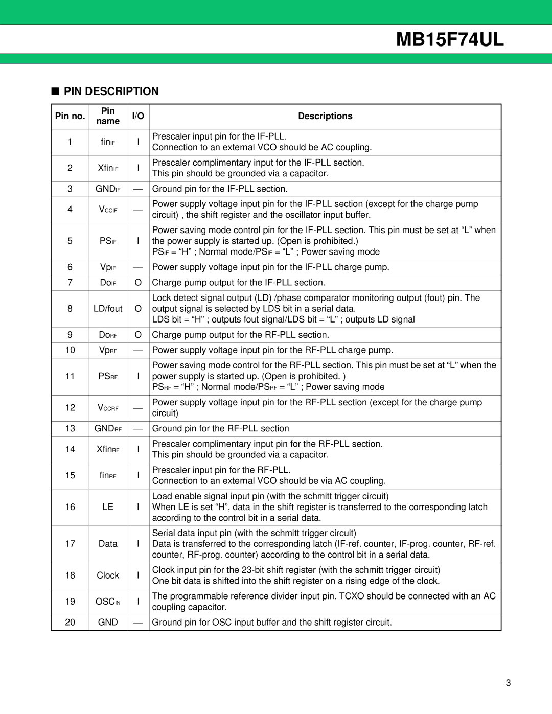
PIN DESCRIPTION

Pin no.

Pin

I/O

Descriptions

name


1

finIF

I

Prescaler input pin for the IF-PLL.

Connection to an external VCO should be AC coupling.


2

XfinIF

I

Prescaler complimentary input for the IF-PLL section.

This pin should be grounded via a capacitor.


3

GNDIF

Ground pin for the IF-PLL section.


4

VCCIF

Power supply voltage input pin for the IF-PLL section (except for the charge pump

circuit) , the shift register and the oscillator input buffer.


Power saving mode control pin for the IF-PLL section. This pin must be set at “L” when

5

PSIF

I

the power supply is started up. (Open is prohibited.)


PSIF = “H” ; Normal mode/PS IF = “L” ; Power saving mode


6

VpIF

Power supply voltage input pin for the IF-PLL charge pump.


7

DoIF

O

Charge pump output for the IF-PLL section.


Lock detect signal output (LD) /phase comparator monitoring output (fout) pin. The

8

LD/fout

O

output signal is selected by LDS bit in a serial data.


LDS bit = “H” ; outputs fout signal/LDS bit = “L” ; outputs LD signal


9

DoRF

O

Charge pump output for the RF-PLL section.


10

VpRF

Power supply voltage input pin for the RF-PLL charge pump.


Power saving mode control for the RF-PLL section. This pin must be set at “L” when the

11

PSRF

I

power supply is started up. (Open is prohibited. )


PSRF = “H” ; Normal mode/PS RF = “L” ; Power saving mode


12

VCCRF

Power supply voltage input pin for the RF-PLL section (except for the charge pump

circuit)


13

GNDRF

Ground pin for the RF-PLL section


14

XfinRF

I

Prescaler complimentary input pin for the RF-PLL section.

This pin should be grounded via a capacitor.


15

finRF

I

Prescaler input pin for the RF-PLL.

Connection to an external VCO should be via AC coupling.


Load enable signal input pin (with the schmitt trigger circuit)

16

LE

I

When LE is set “H”, data in the shift register is transferred to the corresponding latch


according to the control bit in a serial data.


Serial data input pin (with the schmitt trigger circuit)

17

Data

I

Data is transferred to the corresponding latch (IF-ref. counter, IF-prog. counter, RF-ref.


counter, RF-prog. counter) according to the control bit in a serial data.


18

Clock

I

Clock input pin for the 23-bit shift register (with the schmitt trigger circuit)

One bit data is shifted into the shift register on a rising edge of the clock.


19

OSCIN

I

The programmable reference divider input pin. TCXO should be connected with an AC

coupling capacitor.


20

GND

Ground pin for OSC input buffer and the shift register circuit.


3

Page 3
Image 3
Fujitsu MB15F74UL manual PIN Description, Pin no Descriptions

MB15F74UL specifications

The Fujitsu MB15F74UL stands out in the realm of advanced microcontroller units, primarily designed for versatile communication applications. This device is well-suited for industrial automation, robotics, and automotive-related tasks, making it an integral part of modern embedded systems.

One of the MB15F74UL's main features is its ultra-low power consumption, which allows it to operate efficiently without draining power resources, making it ideal for battery-powered applications. This attribute ensures that devices can run for extended periods without requiring frequent recharging, thus enhancing their overall usability in realistic scenarios.

The MB15F74UL employs a sophisticated architecture that supports 16-bit operation. This design not only increases processing speed but also allows for a greater range of data processing and storage, enabling engineers to develop more complex applications. Its high level of integration combines essential functionalities, reducing the need for additional external components and simplifying circuit design.

Additionally, the microcontroller includes a robust set of communication protocols such as UART, I2C, and SPI, which facilitate seamless connectivity with various peripherals and external devices. This versatility makes the MB15F74UL suitable for numerous applications, from sensor interfaces to data transmission, ensuring efficient operation in demanding environments.

Moreover, the device is equipped with a comprehensive set of input/output pins, enabling users to tailor configurations to meet specific project needs. This flexibility facilitates the design of customized solutions, making it an attractive choice for engineers and developers.

In terms of characteristics, the Fujitsu MB15F74UL incorporates built-in memory options, including EEPROM and RAM, further amplifying its capability for data handling and storage. The device's operating temperature range enhances its reliability in harsh industrial conditions, ensuring stable performance even in extreme environments.

Overall, the Fujitsu MB15F74UL embodies a blend of energy efficiency, communication versatility, and robust processing power, making it an excellent choice for a diverse range of embedded systems. Its advanced technology and features cater to the demands of contemporary applications, providing engineers with the tools necessary to innovate and expand their technological horizons.