Pub. | |
Model | Page: 5 of 15 |
Block Diagram
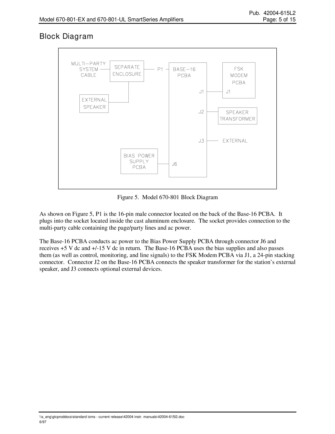
Figure 5. Model 670-801 Block Diagram
As shown on Figure 5, P1 is the 16-pin male connector located on the back of the Base-16 PCBA. It plugs into the socket located inside the cast aluminum enclosure. The socket provides connection to the multi-party cable containing the page/party lines and ac power.
The Base-16 PCBA conducts ac power to the Bias Power Supply PCBA through connector J6 and receives +5 V dc and +/-15 V dc in return. The Base-16 PCBA uses the bias supplies and also passes them (as well as control, monitoring, and line signals) to the FSK Modem PCBA via J1, a 24-pin stacking connector. Connector J2 on the Base-16 PCBA connects the speaker transformer for the station’s external speaker, and J3 connects optional external devices.
\\s_eng\gtcproddocs\standard ioms - current release\42004 instr.